Cryogenic Electronics: Compliance with International Regulations
SEP 29, 20259 MIN READ
Generate Your Research Report Instantly with AI Agent
Patsnap Eureka helps you evaluate technical feasibility & market potential.
Cryogenic Electronics Background and Objectives
Cryogenic electronics represents a frontier technology domain that operates electronic systems at extremely low temperatures, typically below -150°C (123K). The field emerged in the mid-20th century alongside advancements in superconductivity research, with significant acceleration occurring after the discovery of high-temperature superconductors in the 1980s. The fundamental principle driving this technology is the dramatic reduction in electrical resistance and thermal noise at cryogenic temperatures, enabling unprecedented performance improvements in computing speed, energy efficiency, and signal sensitivity.
The evolution of cryogenic electronics has been marked by progressive miniaturization and increasing integration density, paralleling but distinct from conventional electronics development. Recent breakthroughs in quantum computing, space exploration, and medical imaging have catalyzed renewed interest and investment in this specialized field, establishing it as a critical enabling technology for next-generation systems.
The primary objectives of cryogenic electronics development center on addressing several key challenges. First, creating electronic components that maintain functionality and reliability at extremely low temperatures without performance degradation. Second, developing specialized packaging and interconnect technologies that can withstand thermal cycling between ambient and cryogenic temperatures. Third, designing integrated systems that effectively manage the thermal interface between cryogenic and room-temperature environments.
International regulatory frameworks for cryogenic electronics remain fragmented and evolving, with standards bodies such as IEEE, IEC, and ISO only recently beginning to address the unique requirements of these systems. The lack of harmonized global standards presents significant challenges for manufacturers and researchers seeking to commercialize cryogenic electronic technologies across different markets and jurisdictions.
Current technical goals in the field include developing cryogenic-compatible semiconductor technologies beyond silicon, enhancing energy efficiency of cooling systems, extending operational lifetimes of cryogenic components, and establishing standardized testing methodologies. Additionally, there is growing emphasis on creating regulatory compliance pathways that balance innovation with safety and interoperability requirements.
The intersection of cryogenic electronics with quantum technologies has established a particularly promising trajectory, with quantum computing representing perhaps the most visible application. However, the technology also shows tremendous potential in areas including ultra-sensitive instrumentation, medical diagnostics, space-based communications, and next-generation high-performance computing architectures that could dramatically reduce data center energy consumption.
Market Analysis for Cryogenic Electronic Applications
The cryogenic electronics market is experiencing significant growth, driven by advancements in quantum computing, medical imaging, and space exploration. Current market valuations indicate the global cryogenic electronics sector reached approximately 7.2 billion USD in 2022, with projections suggesting a compound annual growth rate of 8.3% through 2030. This growth trajectory is primarily fueled by substantial investments in quantum computing research and development, with major technology corporations allocating increasing portions of their R&D budgets to this emerging field.
Demand analysis reveals three primary market segments driving adoption: scientific research institutions, technology companies developing quantum computing solutions, and aerospace organizations. Scientific research represents the largest current market share at 42%, followed by quantum computing applications at 31%, and aerospace at 18%. The remaining 9% encompasses various niche applications including medical imaging and particle physics experimentation.
Geographically, North America dominates the market with 38% share, followed by Europe at 29% and Asia-Pacific at 26%. The Asia-Pacific region, particularly China, Japan, and South Korea, demonstrates the fastest growth rate at 10.2% annually, reflecting aggressive national initiatives to develop quantum technology capabilities.
Consumer demand patterns indicate a shift toward more integrated cryogenic systems that combine cooling infrastructure with specialized electronics, reducing overall system complexity and operational costs. This trend is particularly evident in commercial quantum computing applications, where ease of implementation is becoming increasingly important for market adoption.
Market barriers include high initial investment costs, specialized knowledge requirements, and complex regulatory compliance across different jurisdictions. The average cost of implementing cryogenic electronic systems remains prohibitively high for many potential applications, with typical quantum computing installations requiring investments of 10-15 million USD for comprehensive systems.
Future market projections suggest significant growth potential in healthcare applications, particularly in advanced MRI technologies and quantum sensing for medical diagnostics. Additionally, the telecommunications sector is emerging as a potential growth market, with research into superconducting components for next-generation communication networks showing promising early results.
Supply chain analysis reveals critical dependencies on rare materials and specialized manufacturing capabilities, with only a limited number of suppliers capable of meeting the stringent requirements for cryogenic electronic components. This supply constraint represents both a market challenge and an opportunity for new entrants with innovative manufacturing approaches.
Global Technical Challenges in Cryogenic Electronics
The development of cryogenic electronics faces significant global technical challenges that require coordinated international efforts to overcome. One primary challenge is the extreme temperature requirements, with most systems needing to operate at temperatures below 10 Kelvin, and quantum computing applications demanding even lower temperatures approaching absolute zero. These extreme conditions create unprecedented materials science challenges, as conventional electronic components fail at such temperatures.
Thermal management represents another critical challenge, as the interface between cryogenic components and room-temperature control systems creates substantial heat gradients that must be carefully managed. Engineers must develop sophisticated thermal isolation techniques while maintaining electrical connectivity, a complex technical balancing act that few organizations have mastered globally.
Reliability and durability concerns are particularly acute in cryogenic electronics. The thermal cycling between ambient and cryogenic temperatures induces significant mechanical stress on components, interconnects, and packaging materials. This stress often leads to premature failures through mechanisms like thermal fatigue and differential thermal expansion, which are difficult to model and predict accurately across international research platforms.
Energy efficiency presents another formidable challenge. Cooling systems required to maintain cryogenic temperatures consume enormous amounts of energy, making many potential applications commercially unviable. The development of more efficient cooling technologies is essential but requires breakthroughs in thermodynamics and materials science that transcend national research boundaries.
Manufacturing standardization remains elusive in the cryogenic electronics field. The lack of globally accepted fabrication standards and testing protocols hampers international collaboration and technology transfer. Different regions have developed disparate approaches to cryogenic electronics manufacturing, creating compatibility issues and redundant development efforts across the global research community.
Specialized testing infrastructure represents a significant bottleneck. Facilities capable of accurately characterizing electronic components at cryogenic temperatures are scarce worldwide and require substantial investment. This limitation restricts innovation to a small number of well-funded research institutions and companies, primarily concentrated in North America, Europe, and parts of Asia.
Supply chain vulnerabilities further complicate development efforts. Many critical materials and components for cryogenic electronics come from limited sources, creating potential geopolitical dependencies. International tensions can disrupt these supply chains, highlighting the need for diversified sourcing strategies and alternative materials development through global scientific cooperation.
Current Cryogenic Electronics Implementation Solutions
01 Superconducting electronic devices
Cryogenic electronics leverages superconducting materials that exhibit zero electrical resistance at extremely low temperatures. These superconducting devices enable high-speed, low-power computing and signal processing capabilities that are not achievable with conventional semiconductor technologies. Applications include quantum computing, ultra-sensitive detectors, and high-performance computing systems that operate at temperatures near absolute zero.- Superconducting electronic devices: Cryogenic electronics leverages superconducting materials that exhibit zero electrical resistance at extremely low temperatures. These devices include superconducting quantum interference devices (SQUIDs), superconducting processors, and other quantum computing components that operate at temperatures near absolute zero. The superconducting state enables high-speed signal processing, reduced power consumption, and enhanced sensitivity for various applications including quantum computing and precision measurements.
- Cryogenic cooling systems for electronics: Specialized cooling systems are essential for maintaining the ultra-low temperatures required by cryogenic electronic components. These systems employ various refrigeration techniques including liquid helium, liquid nitrogen, pulse tube coolers, and Stirling cycle refrigerators. Advanced thermal management solutions ensure stable operating temperatures while minimizing thermal noise and interference, which is crucial for maintaining the performance of sensitive cryogenic electronic devices.
- Cryogenic electronic packaging and interconnects: The design of electronic packaging for cryogenic environments addresses unique challenges related to thermal contraction, material compatibility, and thermal isolation. Specialized interconnect technologies maintain signal integrity across extreme temperature gradients while minimizing heat leakage into the cold environment. These packaging solutions incorporate materials with matched thermal expansion coefficients and novel connection methods to ensure reliable operation at cryogenic temperatures.
- Cryogenic sensor and detector systems: Sensors and detectors operating at cryogenic temperatures offer significantly improved sensitivity and reduced noise compared to room-temperature counterparts. These include infrared detectors, magnetic field sensors, radiation detectors, and precision measurement instruments. The enhanced performance at low temperatures enables applications in astronomy, particle physics, medical imaging, and security screening where detecting extremely weak signals is critical.
- Cryogenic control and interface electronics: Interface systems bridge the gap between cryogenic electronic components and room-temperature control equipment. These systems include specialized amplifiers, signal converters, and control circuits designed to operate across extreme temperature gradients. Advanced control electronics manage the operation of cryogenic systems while minimizing heat introduction to the cold environment, enabling practical implementation of cryogenic electronic technologies in research and commercial applications.
02 Cryogenic cooling systems for electronics
Specialized cooling systems are essential for maintaining electronic components at cryogenic temperatures. These systems employ various refrigeration techniques including liquid helium/nitrogen circulation, pulse tube coolers, and Stirling cycle refrigerators. Advanced thermal management solutions ensure stable operating temperatures while addressing challenges such as thermal cycling, differential thermal expansion, and efficient heat transfer at extremely low temperatures.Expand Specific Solutions03 Cryogenic electronic packaging and interconnects
Electronic packaging for cryogenic environments requires specialized materials and designs to maintain functionality at extremely low temperatures. These include thermal isolation techniques, specialized substrate materials, and custom interconnect solutions that can withstand thermal cycling between room temperature and cryogenic conditions. The packaging must address challenges such as differential thermal contraction, material property changes, and reliable electrical connections across extreme temperature gradients.Expand Specific Solutions04 Cryogenic sensor and detector technologies
Sensors and detectors operating at cryogenic temperatures offer exceptional sensitivity and performance for specialized applications. These include superconducting quantum interference devices (SQUIDs), transition edge sensors, and various quantum-limited detectors used in scientific research, medical imaging, and security applications. The extreme low-temperature environment enables detection of extremely weak signals with minimal thermal noise interference.Expand Specific Solutions05 Cryogenic computing architectures
Novel computing architectures designed specifically for cryogenic operation leverage the unique properties of materials at extremely low temperatures. These include superconducting logic circuits, Josephson junction-based processors, and specialized memory systems that offer advantages in speed, energy efficiency, and quantum coherence. Cryogenic computing architectures are being developed for next-generation high-performance computing, quantum information processing, and specialized signal processing applications.Expand Specific Solutions
Leading Organizations in Cryogenic Electronics Development
Cryogenic Electronics market is currently in a growth phase, with increasing applications in quantum computing, medical devices, and aerospace sectors. The market size is estimated to be around $2-3 billion, with projected annual growth of 8-10% through 2030. Regarding technological maturity, established players like IBM, Intel, and Northrop Grumman lead with advanced superconducting electronics solutions, while newer entrants such as kiutra GmbH and Montana Instruments are innovating in cryogenic cooling systems. Companies like Delft University of Technology and ID Quantique are advancing quantum applications, while regulatory compliance remains challenging across international markets, particularly for dual-use technologies. Chinese companies including Lenovo and Baidu are rapidly expanding their presence, focusing on indigenous development to address export control restrictions.
International Business Machines Corp.
Technical Solution: IBM has developed comprehensive cryogenic electronics solutions that comply with international regulations across multiple jurisdictions. Their quantum computing systems utilize dilution refrigerators operating at millikelvin temperatures with specialized control electronics designed to meet global electromagnetic compatibility (EMC) standards. IBM's cryogenic systems incorporate helium recovery and recycling technology that addresses international regulations concerning helium conservation, with reported recycling rates exceeding 95% in their quantum computing facilities. The company has pioneered cryogenic CMOS technology that operates at 4K while complying with international semiconductor manufacturing standards and restrictions on hazardous substances under regulations like EU RoHS. IBM's quantum systems feature specialized radiation shielding and electromagnetic isolation that meets international safety standards for both research and commercial applications. Their cryogenic control electronics are designed with modular components that can be certified separately in different regulatory environments, facilitating global deployment of their quantum computing technology. IBM actively participates in international standards committees developing specifications for cryogenic electronic systems, helping shape regulatory frameworks that their systems are designed to meet.
Strengths: Extensive experience integrating cryogenic systems with complex computing architectures; global regulatory compliance team ensures systems meet requirements across multiple jurisdictions; substantial R&D resources enable comprehensive testing for regulatory certification. Weaknesses: Complex systems require significant specialized infrastructure; high operational costs compared to non-cryogenic alternatives; proprietary technologies may create vendor lock-in challenges for customers.
kiutra GmbH
Technical Solution: kiutra has developed a groundbreaking magnetic cooling technology for cryogenic electronics that operates without liquid helium, addressing critical international regulatory concerns about helium scarcity. Their system uses magnetic refrigeration principles to reach temperatures below 4K, employing lanthanide compounds as refrigerants that change temperature when exposed to varying magnetic fields. This technology complies with EU RoHS and REACH regulations by eliminating hazardous substances in their cooling systems. kiutra's approach also aligns with international energy efficiency standards by consuming significantly less power than conventional cryostats, with reported energy savings of up to 80% compared to traditional helium-based systems. Their closed-cycle magnetic refrigeration technology meets international safety standards while providing stable cooling for superconducting electronics and quantum computing applications.
Strengths: Helium-free operation addresses regulatory concerns about strategic resource usage; closed-cycle design eliminates need for cryogen refills, reducing operational costs and compliance issues; lower vibration levels than conventional cryocoolers improves measurement precision. Weaknesses: Limited cooling power compared to larger helium-based systems; relatively new technology with less established track record in long-term industrial applications; higher initial capital investment compared to conventional cooling solutions.
Key Patents and Innovations in Cryogenic Electronics
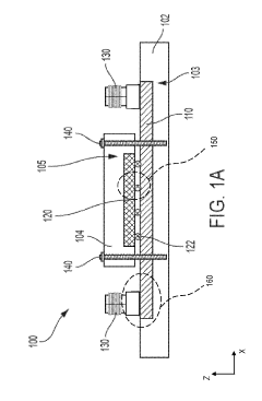
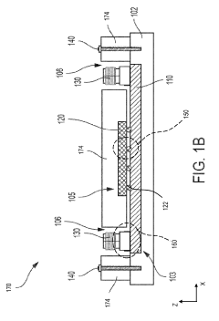
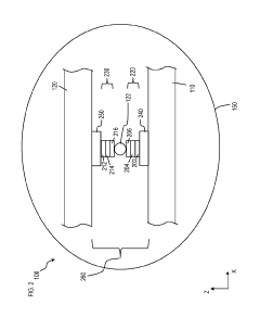
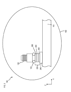
Bump bonded cryogenic chip carrier
PatentActiveUS20190103541A1
Innovation
- A system utilizing thin films with superconducting regions connected by low ohmic solder material with a melting point above 700 degrees Celsius, eliminating the need for intermediary connection mechanisms like wire bonds, and enabling direct electrical and thermal conduction between substrates.
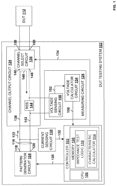
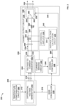
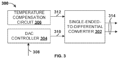
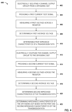
Systems and methods for measuring characteristics of cryogenic electronic devices
PatentActiveUS12019106B2
Innovation
- A system that includes a channel select circuit and a controller to electrically isolate and couple a channel output circuit to a cryogenic device under test, using test current signals to determine impedance characteristics by measuring voltages across resistors in the transmission path, thereby compensating for transmission path nonidealities and impedance mismatches.
International Regulatory Framework for Cryogenic Technologies
The global landscape for cryogenic electronics is shaped by a complex web of international regulations that vary significantly across regions. These regulations primarily focus on safety standards, environmental impact, and technical specifications for cryogenic systems operating at extremely low temperatures. The International Electrotechnical Commission (IEC) has established the IEC 60747 series specifically addressing semiconductor devices, with recent amendments incorporating provisions for cryogenic operation conditions below 77K.
The European Union enforces the most stringent regulatory framework through its Pressure Equipment Directive (PED 2014/68/EU), which governs cryogenic vessels and associated electronic control systems. Additionally, the EU's RoHS (Restriction of Hazardous Substances) and REACH (Registration, Evaluation, Authorization and Restriction of Chemicals) directives impose strict limitations on materials used in cryogenic electronic components, particularly concerning superconducting materials containing heavy metals.
In North America, regulations are primarily administered by the American Society of Mechanical Engineers (ASME) through its Boiler and Pressure Vessel Code Section VIII, which includes provisions for cryogenic equipment. The U.S. Department of Energy has published supplementary guidelines specifically for superconducting electronics in research facilities, while the FDA maintains oversight for medical applications of cryogenic electronics.
The Asia-Pacific region presents a more fragmented regulatory landscape. Japan's High Pressure Gas Safety Act includes specific provisions for cryogenic systems, while China has recently implemented the GB/T 34576-2017 standard addressing safety requirements for superconducting electronic devices. South Korea follows a hybrid approach, adopting elements from both European and American standards.
International transportation of cryogenic electronic components falls under the International Air Transport Association's Dangerous Goods Regulations and the International Maritime Dangerous Goods Code, which mandate specific packaging, labeling, and handling requirements for temperature-sensitive electronic components.
Emerging regulations are increasingly focusing on energy efficiency metrics for cryogenic cooling systems, with the International Organization for Standardization (ISO) developing the ISO 23226 standard specifically addressing energy performance evaluation methods for low-temperature electronic applications. These standards are expected to become more stringent as cryogenic computing applications expand beyond research environments into commercial data centers.
Compliance challenges are particularly acute for multinational corporations developing quantum computing technologies, as they must navigate overlapping and sometimes contradictory regulatory requirements across different jurisdictions while managing proprietary technology concerns in an increasingly competitive global landscape.
Environmental Impact and Sustainability Considerations
The environmental footprint of cryogenic electronics represents a significant consideration in the context of international regulatory compliance. Cooling systems required for maintaining superconducting states consume substantial energy, with traditional cryogenic cooling technologies demanding between 50-100 kW per kilowatt of cooling power at liquid helium temperatures. This energy intensity poses challenges for sustainability goals outlined in frameworks such as the European Green Deal and the UN Sustainable Development Goals.
Refrigerants used in cryogenic systems present another environmental concern. Many traditional coolants contain compounds with high global warming potential (GWP) or ozone depletion potential (ODP). Recent regulations, including the Kigali Amendment to the Montreal Protocol, mandate the phase-down of hydrofluorocarbons (HFCs) commonly used in cooling systems, necessitating transition to more environmentally benign alternatives like helium or hydrogen.
Material sustainability in cryogenic electronics encompasses both resource scarcity and end-of-life considerations. Rare earth elements and precious metals essential for superconducting components face supply constraints and geopolitical challenges. The European Union's Critical Raw Materials Act and similar regulations worldwide increasingly require manufacturers to document material sourcing and implement recycling strategies for these valuable resources.
Lifecycle assessment (LCA) methodologies are becoming mandatory under various international frameworks. The ISO 14040 series provides standardized approaches for evaluating environmental impacts throughout a product's lifecycle. For cryogenic electronics, this includes accounting for the embodied carbon in specialized materials, manufacturing energy requirements, operational energy consumption, and end-of-life management.
Energy efficiency improvements represent a promising pathway toward regulatory compliance. Recent advances in cryocooler technology have demonstrated efficiency gains of 15-25% compared to previous generations. The implementation of waste heat recovery systems can further improve overall system efficiency by repurposing thermal energy that would otherwise be dissipated.
Circular economy principles are increasingly embedded in international regulations affecting cryogenic electronics. The EU's Circular Economy Action Plan and similar initiatives worldwide emphasize design for disassembly, component reuse, and material recovery. Manufacturers must now consider how superconducting components and specialized materials can be recovered and reintegrated into production cycles, reducing virgin material demand and minimizing waste generation.
Unlock deeper insights with Patsnap Eureka Quick Research — get a full tech report to explore trends and direct your research. Try now!
Generate Your Research Report Instantly with AI Agent
Supercharge your innovation with Patsnap Eureka AI Agent Platform!