Cryogenic Electronics: Patents, Trends, and Technical Innovations
SEP 29, 20259 MIN READ
Generate Your Research Report Instantly with AI Agent
Patsnap Eureka helps you evaluate technical feasibility & market potential.
Cryogenic Electronics Background and Objectives
Cryogenic electronics represents a specialized field at the intersection of electrical engineering and low-temperature physics, focusing on the development and application of electronic systems that operate at extremely low temperatures, typically below 123K (-150°C). The evolution of this technology dates back to the mid-20th century, with significant advancements occurring in parallel with developments in superconductivity research. The field has progressed from fundamental scientific exploration to practical applications in quantum computing, space exploration, and advanced sensing technologies.
The technological trajectory of cryogenic electronics has been characterized by continuous innovation in materials science, circuit design, and fabrication techniques. Early developments centered on basic superconducting devices, while recent advances have expanded to include complex integrated circuits capable of functioning at temperatures approaching absolute zero. This progression has been driven by the unique advantages offered by low-temperature operation, including reduced thermal noise, increased energy efficiency, and access to quantum mechanical phenomena.
Current research objectives in cryogenic electronics focus on overcoming several critical challenges. These include developing materials with improved performance at low temperatures, designing more energy-efficient cooling systems, and creating interface technologies that bridge cryogenic components with room-temperature electronics. Additionally, there is significant emphasis on miniaturization and integration to enable more compact and powerful cryogenic systems.
The field aims to achieve breakthroughs in several key areas: enhancing the reliability and longevity of cryogenic electronic components; reducing the power consumption of cooling systems; improving signal integrity across temperature gradients; and developing standardized design methodologies for cryogenic circuits. These objectives are crucial for enabling the next generation of quantum computers, ultra-sensitive detectors, and space-based electronics.
Long-term goals include the creation of complete cryogenic computing platforms that can outperform conventional electronics in specific applications, particularly those requiring extreme sensitivity or quantum coherence. The development of room-temperature superconductors would represent a paradigm shift, potentially eliminating the need for complex cooling systems and dramatically expanding the practical applications of cryogenic electronics.
The field is increasingly interdisciplinary, drawing expertise from electrical engineering, materials science, quantum physics, and thermal management. This convergence of disciplines is expected to accelerate innovation and lead to novel applications across multiple industries, from healthcare to telecommunications to national security.
Market Analysis for Cryogenic Electronic Applications
The cryogenic electronics market is experiencing significant growth driven by advancements in quantum computing, superconducting technologies, and specialized research applications. Current market estimates value the global cryogenic electronics sector at approximately $2.3 billion, with projections indicating a compound annual growth rate (CAGR) of 7.8% through 2028. This growth trajectory is primarily fueled by substantial investments in quantum computing research from both private corporations and government entities worldwide.
The market segmentation reveals distinct application categories with varying growth potentials. Quantum computing represents the largest and fastest-growing segment, accounting for nearly 40% of the total market value. This dominance stems from the critical role cryogenic electronics play in qubit control systems and readout electronics, where operating temperatures below 100 mK are essential for maintaining quantum coherence.
Superconducting electronics form the second-largest market segment, comprising approximately 25% of the market. This includes applications in medical imaging systems (particularly MRI equipment), particle accelerators, and emerging superconducting computing architectures. The medical imaging subsegment alone generates annual revenues exceeding $300 million.
Space and defense applications constitute roughly 20% of the market, with growing demand for radiation-hardened, low-power cryogenic systems for satellite communications, deep space exploration, and specialized military applications. The remaining market share is distributed across scientific research instrumentation, cryogenic sensors, and emerging applications in quantum sensing.
Geographically, North America leads the market with approximately 45% share, driven by substantial research funding and the presence of major technology companies investing in quantum technologies. Europe follows with 30% market share, particularly strong in scientific research applications. The Asia-Pacific region, while currently representing about 20% of the market, is experiencing the fastest regional growth rate at 9.5% annually, primarily led by China's aggressive investments in quantum technologies and Japan's established superconducting electronics industry.
Customer segmentation reveals three primary buyer categories: research institutions (35%), technology corporations (40%), and government/defense entities (25%). The technology corporations segment is growing most rapidly as companies like IBM, Google, Microsoft, and Intel increase investments in quantum computing infrastructure. Market analysts project that by 2026, this segment will represent over 50% of total market value as quantum computing moves closer to commercial viability.
Current Challenges in Cryogenic Electronics Development
Despite significant advancements in cryogenic electronics over recent decades, the field continues to face substantial technical challenges that impede widespread commercial adoption. Material behavior at extremely low temperatures remains a primary obstacle, as conventional semiconductor materials exhibit altered electrical properties when cooled to cryogenic temperatures. Silicon, the backbone of modern electronics, experiences carrier freeze-out below approximately 50K, necessitating complex doping strategies or alternative materials that can maintain functionality at temperatures approaching absolute zero.
Interconnect technologies present another critical challenge, as the thermal contraction coefficients of different materials create mechanical stress at interfaces during cooling cycles. This stress often leads to connection failures, reduced reliability, and shortened operational lifespans of cryogenic electronic systems. The development of compatible interconnect solutions that can withstand repeated thermal cycling while maintaining electrical integrity remains an active area of research.
Power dissipation management constitutes a significant hurdle in cryogenic electronics development. While operating at low temperatures reduces certain thermal noise effects, any heat generated by active components requires extraction through sophisticated cooling systems. The energy cost of removing heat at cryogenic temperatures is exponentially higher than at room temperature, creating a fundamental efficiency challenge for system designers.
Integration complexity between room-temperature and cryogenic components presents substantial engineering difficulties. Most cryogenic systems require some interface with room-temperature electronics for control and data acquisition, necessitating specialized transition regions that can bridge these extreme temperature differentials without compromising performance or reliability.
Manufacturing scalability remains perhaps the most significant barrier to widespread adoption. Current fabrication processes for cryogenic electronics often involve custom materials, specialized equipment, and low-volume production techniques that result in prohibitively high costs. The absence of standardized manufacturing protocols comparable to those in conventional semiconductor fabrication limits economies of scale and restricts application to niche markets where performance requirements justify the premium costs.
Reliability testing methodologies for cryogenic electronics are still evolving, with limited industry standards and insufficient long-term performance data. The extreme operating conditions make accelerated life testing particularly challenging, complicating efforts to predict system longevity and maintenance requirements accurately.
Packaging solutions specifically designed for cryogenic environments remain underdeveloped, with few commercial options that adequately address thermal management, electromagnetic interference shielding, and mechanical stability at extremely low temperatures. This gap in the component ecosystem forces many developers to create custom packaging solutions, further increasing development costs and time-to-market.
State-of-the-Art Cryogenic Electronic Solutions
01 Cryogenic cooling systems for electronic components
Specialized cooling systems designed to maintain electronic components at cryogenic temperatures for improved performance. These systems utilize various refrigeration techniques to achieve ultra-low temperatures necessary for superconducting electronics and quantum computing applications. The cooling infrastructure includes circulation systems, thermal interfaces, and insulation to maintain stable cryogenic environments while managing heat loads from electronic operations.- Superconducting electronic devices: Cryogenic electronics leverages superconducting materials that exhibit zero electrical resistance at extremely low temperatures. These devices include superconducting quantum interference devices (SQUIDs), superconducting qubits, and other quantum computing components that operate at temperatures near absolute zero. The superconducting state enables high-speed, low-power operation with minimal thermal noise, making these devices ideal for quantum computing applications and ultra-sensitive measurements.
- Cryogenic cooling systems for electronics: Specialized cooling systems are essential for maintaining electronic components at cryogenic temperatures. These systems include closed-cycle refrigerators, liquid helium/nitrogen cooling apparatus, pulse tube coolers, and dilution refrigerators. Advanced thermal management techniques ensure stable operating temperatures while minimizing vibration and electromagnetic interference that could disrupt sensitive electronic operations. These cooling solutions enable the practical implementation of cryogenic electronics in various applications.
- Cryogenic electronic packaging and interconnects: Specialized packaging solutions are designed to maintain signal integrity and thermal performance at extremely low temperatures. These include thermal isolation techniques, specialized materials with matched thermal expansion coefficients, and vacuum-sealed enclosures. Advanced interconnect technologies address challenges such as thermal contraction, material property changes, and thermal gradients between cryogenic components and room-temperature interfaces, ensuring reliable operation under extreme temperature conditions.
- Cryogenic computing architectures: Computing systems designed specifically for cryogenic operation leverage the unique properties of materials at ultra-low temperatures. These architectures include specialized memory systems, logic circuits, and data processing units optimized for cryogenic environments. The designs focus on minimizing heat generation, maximizing computational efficiency, and leveraging quantum effects for enhanced performance. These systems often integrate with quantum computing elements to create hybrid classical-quantum computing platforms.
- Cryogenic sensors and measurement systems: Ultra-sensitive detection and measurement systems operate at cryogenic temperatures to achieve unprecedented precision. These include magnetic field sensors, radiation detectors, and gravitational wave detectors. The extreme cold reduces thermal noise and enables detection of extremely weak signals that would be obscured at higher temperatures. Applications include medical imaging, astronomical observations, particle physics research, and security screening, where the enhanced sensitivity provides significant advantages over conventional technologies.
02 Superconducting electronic circuits and devices
Electronic circuits and devices designed to operate at cryogenic temperatures to leverage superconductivity properties. These include superconducting processors, memory elements, and interconnects that exhibit zero electrical resistance at cryogenic temperatures. The technology enables higher processing speeds, reduced power consumption, and improved signal integrity compared to conventional electronics operating at room temperature.Expand Specific Solutions03 Thermal management for cryogenic electronic systems
Specialized thermal management solutions for addressing the unique challenges of cryogenic electronic systems. These include thermal interfaces, heat shields, and isolation techniques to maintain temperature stability and prevent thermal interference between components operating at different temperature regimes. Advanced materials and structures are employed to manage thermal gradients and heat dissipation in extremely cold environments.Expand Specific Solutions04 Quantum computing hardware at cryogenic temperatures
Hardware architectures specifically designed for quantum computing applications operating at cryogenic temperatures. These systems include qubit arrays, control electronics, and measurement systems that function in extreme cold to maintain quantum coherence. The designs address challenges of signal integrity, thermal isolation, and electromagnetic interference while enabling the precise control needed for quantum operations.Expand Specific Solutions05 Cryogenic electronic packaging and interconnects
Specialized packaging solutions and interconnect technologies designed to function reliably at cryogenic temperatures. These include materials and structures that accommodate thermal contraction, maintain electrical performance, and provide mechanical stability across extreme temperature ranges. Advanced interconnect technologies enable high-speed signal transmission while minimizing thermal leakage between temperature stages in cryogenic systems.Expand Specific Solutions
Leading Companies and Research Institutions in Cryogenics
Cryogenic Electronics is currently in a transitional phase from research to early commercialization, with the global market estimated at $1.2-1.5 billion and projected to grow significantly as quantum computing applications expand. The technology maturity varies across applications, with superconducting quantum computing showing the most advancement. Key players shaping the competitive landscape include IBM, which leads in quantum processor development; Microsoft Technology Licensing focusing on software and control systems; specialized quantum hardware providers like D-Wave Systems and PsiQuantum; and cryogenic infrastructure companies such as Montana Instruments and kiutra GmbH. The ecosystem is further supported by research institutions like Naval Research Laboratory and MIT, creating a diverse competitive environment where strategic partnerships between hardware, software, and infrastructure providers are becoming increasingly important.
Microsoft Technology Licensing LLC
Technical Solution: Microsoft has developed an innovative approach to cryogenic electronics focused on quantum computing applications. Their Azure Quantum program incorporates topological qubits that require ultra-low temperatures for operation. Microsoft's cryogenic electronics strategy centers on developing a complete quantum stack, from hardware to software, with specialized cryogenic control systems that can operate reliably at millikelvin temperatures[4]. Their patents cover novel cryogenic memory architectures that maintain data integrity at extreme temperatures and specialized interconnect technologies that minimize thermal loading. Microsoft has pioneered a hybrid approach that strategically places certain control electronics at different temperature stages within the cryogenic system, optimizing for both performance and power efficiency[5]. Their innovations include specialized cryogenic CMOS designs that can operate at 4K while consuming minimal power, and advanced packaging techniques that accommodate the significant thermal contraction that occurs when cooling to cryogenic temperatures.
Strengths: Comprehensive system-level approach integrating hardware and software; strong focus on scalability for future quantum systems; significant R&D resources and partnerships with leading academic institutions. Weaknesses: Still developing physical qubit implementations compared to competitors; challenges in achieving reliable operation of complex control electronics at cryogenic temperatures; high infrastructure requirements for deployment.
PsiQuantum Corp.
Technical Solution: PsiQuantum is developing photonic quantum computing technology that relies on cryogenic electronics for control and readout systems. Their approach uses silicon photonics operating at cryogenic temperatures to implement quantum logic, with specialized cryogenic detectors for measuring single photons. PsiQuantum's architecture incorporates superconducting nanowire single-photon detectors (SNSPDs) that must operate at temperatures below 2K to achieve the necessary sensitivity and timing resolution[6]. Their patents cover novel techniques for integrating these detectors with silicon photonic circuits while maintaining thermal isolation. PsiQuantum has developed specialized cryogenic packaging solutions that allow optical signals to enter the cryogenic environment with minimal thermal impact, and custom cryogenic electronic circuits for detector bias and signal processing. Their innovations include multiplexed readout systems that can process signals from thousands of detectors simultaneously, critical for scaling their photonic quantum computing approach.
Strengths: Unique photonic approach potentially offering advantages in scalability; integration of silicon photonics with cryogenic electronics expertise; strong focus on manufacturing scalability using semiconductor industry processes. Weaknesses: Complex integration challenges between photonic and electronic components; high sensitivity to thermal and mechanical disturbances; requires advancement in both photonic and cryogenic electronic technologies simultaneously.
Key Patents and Innovations in Cryogenic Electronics
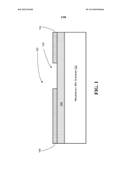
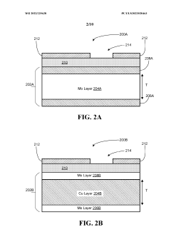
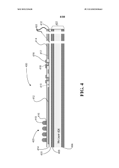
Multilayer superconducting structures for cryogenic electronics
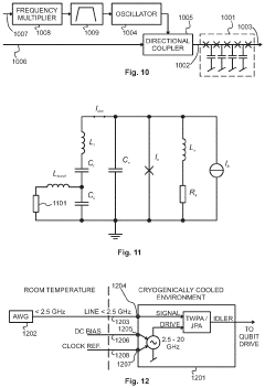
PatentWO2022225628A1
Innovation
- The use of a molybdenum substrate with copper cladding layers, matched to the CTE of cryogenic electronic chips, provides improved thermal conductivity and reduced mechanical stresses, ensuring reliable operation from room temperature to deep cryogenic temperatures by fine-tuning the CTE and thermal conductivity characteristics through layer thickness and purity adjustments.
Cryogenic integrated circuit, integrated module, and arrangement for producing and detecting excitation and readout signals of qubits
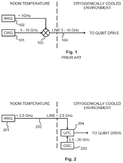
PatentActiveUS12009789B2
Innovation
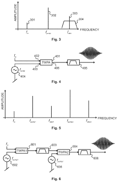
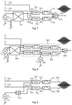
- The use of a cryogenic integrated circuit or module with a travelling wave parametric amplifier or Josephson parametric amplifier for up-conversion of excitation signals within the cryogenically cooled environment, allowing for more efficient frequency conversion and reduced heat load by operating at lower frequencies and integrating multiple components on a single substrate or separate chips for optimized performance.
Materials Science Advancements for Cryogenic Applications
The evolution of cryogenic electronics has been significantly propelled by breakthroughs in materials science. Traditional materials often fail under extreme low-temperature conditions, exhibiting brittleness, thermal contraction issues, and altered electrical properties. Recent advancements have focused on developing novel materials specifically engineered to maintain functionality and reliability at cryogenic temperatures.
Superconducting materials represent one of the most critical areas of development, with high-temperature superconductors (HTS) like YBCO (Yttrium Barium Copper Oxide) and BSCCO (Bismuth Strontium Calcium Copper Oxide) compounds showing remarkable performance improvements. These materials maintain superconductivity at temperatures achievable with liquid nitrogen cooling, significantly reducing operational costs compared to traditional low-temperature superconductors requiring liquid helium.
Specialized substrate materials have emerged as another crucial innovation area. Silicon-on-insulator (SOI) technologies modified for cryogenic applications demonstrate superior performance by minimizing leakage currents and parasitic capacitances at low temperatures. Additionally, sapphire substrates have gained prominence for their excellent thermal conductivity and electrical insulation properties in cryogenic environments.
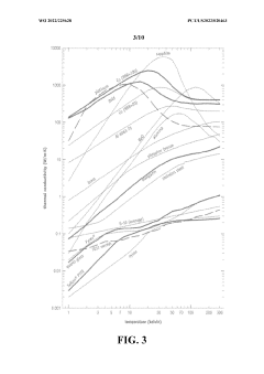
Thermal interface materials (TIMs) designed specifically for cryogenic applications address the critical challenge of efficient heat transfer at low temperatures. Advanced composites incorporating diamond particles, graphene, and specialized metal alloys have demonstrated thermal conductivity values exceeding 2000 W/m·K at cryogenic temperatures, representing a tenfold improvement over previous generations.
Packaging materials have also undergone significant evolution, with ceramic-based packages and specialized polymers replacing traditional epoxy-based encapsulants that become brittle at low temperatures. These new materials maintain mechanical integrity while accommodating thermal contraction mismatches between different components.
Recent patent activity reveals increasing interest in metamaterials and nanostructured composites engineered at the molecular level to exhibit tailored properties at cryogenic temperatures. These include materials with near-zero thermal expansion coefficients and those with programmable electrical conductivity responses to temperature changes, enabling more robust and reliable cryogenic electronic systems.
The convergence of quantum materials science with cryogenic applications has opened new frontiers, with topological insulators and Weyl semimetals showing promise for next-generation cryogenic computing architectures. These materials exhibit unique quantum states that remain coherent at low temperatures, potentially enabling fault-tolerant quantum information processing.
Superconducting materials represent one of the most critical areas of development, with high-temperature superconductors (HTS) like YBCO (Yttrium Barium Copper Oxide) and BSCCO (Bismuth Strontium Calcium Copper Oxide) compounds showing remarkable performance improvements. These materials maintain superconductivity at temperatures achievable with liquid nitrogen cooling, significantly reducing operational costs compared to traditional low-temperature superconductors requiring liquid helium.
Specialized substrate materials have emerged as another crucial innovation area. Silicon-on-insulator (SOI) technologies modified for cryogenic applications demonstrate superior performance by minimizing leakage currents and parasitic capacitances at low temperatures. Additionally, sapphire substrates have gained prominence for their excellent thermal conductivity and electrical insulation properties in cryogenic environments.
Thermal interface materials (TIMs) designed specifically for cryogenic applications address the critical challenge of efficient heat transfer at low temperatures. Advanced composites incorporating diamond particles, graphene, and specialized metal alloys have demonstrated thermal conductivity values exceeding 2000 W/m·K at cryogenic temperatures, representing a tenfold improvement over previous generations.
Packaging materials have also undergone significant evolution, with ceramic-based packages and specialized polymers replacing traditional epoxy-based encapsulants that become brittle at low temperatures. These new materials maintain mechanical integrity while accommodating thermal contraction mismatches between different components.
Recent patent activity reveals increasing interest in metamaterials and nanostructured composites engineered at the molecular level to exhibit tailored properties at cryogenic temperatures. These include materials with near-zero thermal expansion coefficients and those with programmable electrical conductivity responses to temperature changes, enabling more robust and reliable cryogenic electronic systems.
The convergence of quantum materials science with cryogenic applications has opened new frontiers, with topological insulators and Weyl semimetals showing promise for next-generation cryogenic computing architectures. These materials exhibit unique quantum states that remain coherent at low temperatures, potentially enabling fault-tolerant quantum information processing.
Quantum Computing Integration with Cryogenic Electronics
The integration of quantum computing with cryogenic electronics represents a critical frontier in advancing quantum information processing capabilities. Quantum computers require ultra-low temperatures to maintain quantum coherence and minimize error rates, typically operating at millikelvin temperatures. This necessitates specialized cryogenic electronic systems that can function reliably in extreme cold while interfacing with quantum bits (qubits).
Recent patent activity reveals significant innovation in cryogenic control electronics, with major technology companies and research institutions focusing on scalable architectures for qubit control. Intel, IBM, and Google have filed patents addressing the challenges of signal integrity and heat management in cryogenic environments, with particular emphasis on multiplexing techniques that reduce wiring complexity and thermal load.
The technical convergence between quantum computing and cryogenic electronics has accelerated development of superconducting digital logic, such as Rapid Single Flux Quantum (RSFQ) and Energy-Efficient RSFQ variants. These technologies offer promising solutions for quantum control systems by providing high-speed, low-power digital processing capabilities at cryogenic temperatures.
A significant trend observed in patent literature is the development of integrated cryogenic CMOS (cryo-CMOS) technologies. These innovations aim to place control electronics in closer proximity to quantum processors, reducing latency and improving system performance. Horse Ridge, Intel's cryogenic control chip, exemplifies this approach by integrating multiple control functions into a single chip operating at 4 Kelvin.
Technical challenges being addressed include signal fidelity preservation across temperature gradients, power dissipation management, and materials compatibility. Novel approaches utilizing superconducting interconnects and specialized packaging techniques are emerging to overcome these barriers.
The quantum-cryogenic interface represents a particularly active area of innovation, with patents describing specialized transducers and signal conversion methodologies. These developments enable efficient translation between the classical electronic domain and quantum states, a crucial requirement for practical quantum computing systems.
Looking forward, the co-design of quantum processors and their cryogenic electronic infrastructure is becoming increasingly important. Patents indicate a trend toward holistic system architectures that consider thermal budgets, signal integrity, and scalability from the outset, rather than treating quantum and classical components as separate development challenges.
Unlock deeper insights with Patsnap Eureka Quick Research — get a full tech report to explore trends and direct your research. Try now!
Generate Your Research Report Instantly with AI Agent
Supercharge your innovation with Patsnap Eureka AI Agent Platform!