Cryogenic Electronics: Strategies for Minimizing Thermal Noise
SEP 29, 20259 MIN READ
Generate Your Research Report Instantly with AI Agent
Patsnap Eureka helps you evaluate technical feasibility & market potential.
Cryogenic Electronics Background and Objectives
Cryogenic electronics represents a frontier domain in semiconductor technology that operates at extremely low temperatures, typically below 120K (-153°C). The field emerged in the mid-20th century with the development of superconducting materials and has evolved significantly over the past decades. The fundamental principle driving this technology is the reduction of thermal noise and energy dissipation that occurs at ultra-low temperatures, enabling electronic systems with unprecedented performance characteristics.
The evolution of cryogenic electronics has been marked by several significant milestones. Initial research focused primarily on superconducting materials and their applications in sensitive detectors. By the 1980s, the development of Josephson junctions and SQUID (Superconducting Quantum Interference Device) magnetometers demonstrated the practical potential of superconducting electronics. The 1990s and early 2000s saw the integration of cryogenic technologies with conventional semiconductor approaches, creating hybrid systems that leveraged the advantages of both domains.
Recent technological trends indicate a convergence of cryogenic electronics with quantum computing, where ultra-low temperature operation is essential for maintaining quantum coherence. Additionally, there is growing interest in cryogenic CMOS technologies that can operate reliably at temperatures approaching absolute zero, offering significant advantages for space exploration, high-performance computing, and sensitive scientific instrumentation.
The primary objective of cryogenic electronics research is to develop electronic systems that can function optimally at extremely low temperatures while effectively minimizing thermal noise. This encompasses several specific goals: designing semiconductor devices with stable electrical characteristics at cryogenic temperatures; creating specialized circuit architectures that capitalize on the unique physics of low-temperature operation; developing thermal management solutions that maintain stable cryogenic environments; and establishing reliable interconnect technologies that can withstand thermal cycling between ambient and cryogenic temperatures.
Furthermore, the field aims to address the fundamental challenge of thermal noise reduction through innovative material science approaches, novel device structures, and advanced signal processing techniques. By minimizing thermal noise, cryogenic electronics can achieve unprecedented levels of sensitivity in sensing applications, reduced error rates in computing systems, and extended operational lifetimes for space-based electronics.
The ultimate technological objective is to create a comprehensive ecosystem of cryogenic electronic components and systems that can enable next-generation applications in quantum computing, space exploration, medical imaging, and scientific research, where the performance advantages of low-temperature operation provide transformative capabilities beyond what is possible with conventional room-temperature electronics.
Market Analysis for Low-Temperature Electronic Applications
The cryogenic electronics market is experiencing significant growth driven by advancements in quantum computing, space exploration, and scientific research applications. Current market valuations indicate the global cryogenic equipment market exceeds $2 billion, with specialized cryogenic electronics components representing a rapidly expanding segment projected to grow at a compound annual rate of 7-9% through 2030.
Low-temperature electronic applications span multiple sectors, with quantum computing emerging as the primary commercial driver. Major technology corporations including IBM, Google, and Intel have invested hundreds of millions in developing quantum systems that require operating temperatures near absolute zero. This investment trend is expected to continue as quantum computing approaches practical commercial applications in fields such as cryptography, material science, and pharmaceutical development.
The scientific research sector represents another substantial market, with high-energy physics facilities, astronomical observatories, and medical imaging systems requiring specialized cryogenic electronics. The CERN Large Hadron Collider alone utilizes thousands of cryogenic sensors and control systems, while medical MRI machines constitute a stable market segment valued at approximately $7 billion globally.
Space exploration presents a growing application area as both government agencies and private companies expand deep space missions. These environments naturally expose electronics to extreme cold, creating demand for components specifically designed to function reliably at cryogenic temperatures without additional heating requirements, thereby reducing power consumption and extending mission durations.
Superconducting electronics represent a specialized but expanding market segment. Applications include ultra-sensitive magnetic sensors (SQUIDs), high-performance filters for telecommunications, and next-generation computing architectures. While currently niche, this segment shows potential for disruptive growth as manufacturing processes mature and costs decrease.
Customer requirements across these markets consistently emphasize reliability under temperature cycling, minimal self-heating, and compatibility with standard interface protocols. The price sensitivity varies significantly by sector, with commercial applications demanding cost-effective solutions while specialized scientific and defense applications prioritizing performance over cost considerations.
Regional analysis shows North America leading market development due to concentrated quantum computing research and space exploration initiatives. Europe follows closely with significant investments in scientific infrastructure, while Asia-Pacific regions are rapidly expanding their market presence through strategic government investments in quantum technologies and cryogenic research facilities.
Current Challenges in Thermal Noise Reduction
Despite significant advancements in cryogenic electronics, thermal noise reduction remains a formidable challenge that impedes the full realization of quantum computing and superconducting technologies. The fundamental limitation stems from Johnson-Nyquist noise, which persists even at extremely low temperatures, creating a noise floor that degrades signal integrity in sensitive quantum circuits.
Material interface issues present a major obstacle in thermal noise management. The thermal expansion coefficient mismatch between different materials used in cryogenic systems creates mechanical stress at interfaces during cooling cycles. These stresses can generate additional noise sources and compromise the integrity of electrical connections, particularly in complex multi-material quantum processor architectures.
Heat dissipation represents another critical challenge. Even minimal power dissipation in cryogenic environments can cause significant temperature gradients, leading to thermal fluctuations that manifest as noise. Current cooling technologies struggle to efficiently extract heat from densely packed cryogenic circuits without introducing additional electromagnetic interference or vibration-induced noise.
Interconnect technologies face unique difficulties at cryogenic temperatures. Traditional interconnect materials and designs optimized for room temperature operation exhibit altered electrical characteristics when cooled to millikelvin ranges. This results in impedance mismatches, signal reflections, and increased noise coupling between components, degrading overall system performance.
Measurement instrumentation introduces its own set of challenges. Room-temperature measurement equipment connected to cryogenic systems can inject thermal noise through cables and connections. The development of fully cryogenic measurement systems remains limited by the availability of low-noise, low-power cryogenic amplifiers and analog-to-digital converters that can operate reliably at extreme temperatures.
Scaling issues become increasingly problematic as cryogenic electronic systems grow in complexity. Larger quantum processors require more control lines and readout channels, each potentially introducing additional thermal load and noise pathways. Current dilution refrigerator technologies face practical limits in cooling capacity that constrain the scalability of quantum computing architectures.
Fabrication process variations introduce inconsistencies in device performance that manifest as noise. At cryogenic temperatures, even minor impurities or structural defects in semiconductor materials can significantly impact electron mobility and create localized heating effects that contribute to thermal noise. Advanced fabrication techniques with atomic-level precision are needed but remain technically challenging to implement at production scales.
Current Thermal Noise Mitigation Techniques
01 Cryogenic cooling systems for electronic devices
Specialized cooling systems designed to maintain electronic components at extremely low temperatures to reduce thermal noise and improve performance. These systems often employ liquid nitrogen, helium, or other cryogenic fluids to achieve temperatures near absolute zero, which significantly reduces electron thermal motion and associated noise in sensitive electronic circuits.- Superconducting quantum devices for low thermal noise electronics: Superconducting materials and quantum devices operate at cryogenic temperatures to minimize thermal noise, enabling high-sensitivity measurements and quantum information processing. These systems leverage quantum effects that emerge at extremely low temperatures to achieve noise levels far below conventional electronics. The superconducting state eliminates electrical resistance and associated Johnson noise, making these systems ideal for applications requiring ultra-low noise performance.
- Cryogenic cooling systems for electronic noise reduction: Specialized cooling systems are designed to maintain electronic components at cryogenic temperatures, significantly reducing thermal noise. These systems employ various cooling technologies including liquid helium/nitrogen circulation, pulse tube refrigerators, and adiabatic demagnetization refrigerators. Advanced thermal management techniques ensure stable operating temperatures and efficient heat extraction, which is critical for maintaining the low-noise environment required by sensitive cryogenic electronics.
- Low-temperature semiconductor devices and circuits: Semiconductor devices specifically designed for cryogenic operation exhibit significantly reduced thermal noise compared to room-temperature counterparts. These include specialized transistors, amplifiers, and integrated circuits that maintain functionality at extremely low temperatures while benefiting from reduced carrier scattering and leakage currents. The devices often incorporate unique doping profiles, material compositions, and circuit topologies optimized for cryogenic performance, enabling improved signal-to-noise ratios in scientific instrumentation and quantum computing applications.
- Thermal noise measurement and characterization at cryogenic temperatures: Specialized techniques and equipment are used to accurately measure and characterize thermal noise in cryogenic electronic systems. These methods include ultra-sensitive amplification chains, correlation techniques, and precision temperature control to isolate and quantify various noise sources. Advanced measurement protocols help distinguish between thermal noise, 1/f noise, and other noise mechanisms, enabling the development of improved low-noise cryogenic electronic components and systems.
- Shielding and isolation techniques for cryogenic electronics: Specialized shielding and isolation methods protect cryogenic electronic systems from external electromagnetic interference and thermal radiation, which can introduce noise. These techniques include multi-layer magnetic shielding, careful grounding schemes, thermal radiation barriers, and vibration isolation systems. Proper cable design and filtering are also critical to prevent noise coupling between different temperature stages in cryogenic systems, ensuring that the intrinsic low thermal noise advantage of cryogenic operation is preserved.
02 Superconducting quantum devices with thermal noise mitigation
Quantum electronic devices that operate at cryogenic temperatures to leverage superconductivity properties for reduced thermal noise. These devices include superconducting qubits, SQUID magnetometers, and other quantum sensors that require ultra-low temperatures to maintain quantum coherence and minimize thermal interference in signal processing and measurement applications.Expand Specific Solutions03 Thermal insulation and shielding techniques for cryogenic electronics
Advanced insulation and shielding methods specifically designed to protect cryogenic electronic components from external heat sources and electromagnetic interference. These techniques include multi-layer vacuum insulation, radiation shields, and specialized materials that maintain the thermal integrity of cryogenic systems while allowing necessary electrical connections to room-temperature environments.Expand Specific Solutions04 Low-noise amplifiers and signal processing for cryogenic applications
Specialized electronic amplifiers and signal processing circuits designed to operate at cryogenic temperatures with minimal thermal noise contribution. These components are engineered with carefully selected materials and circuit topologies to maintain signal integrity in extreme cold, often incorporating HEMT transistors, SiGe devices, or superconducting elements to achieve noise temperatures approaching quantum limits.Expand Specific Solutions05 Thermal noise measurement and characterization at cryogenic temperatures
Methods and systems for accurately measuring, characterizing, and modeling thermal noise in electronic components at cryogenic temperatures. These approaches include specialized test equipment, calibration techniques, and theoretical models that account for quantum effects that become significant at extremely low temperatures, enabling the design of optimized low-noise cryogenic electronic systems.Expand Specific Solutions
Leading Organizations in Cryogenic Electronics Research
Cryogenic Electronics is currently in a transitional phase from research to early commercialization, with the global market estimated at $500-700 million and projected to grow significantly as quantum computing advances. The technology maturity varies across applications, with superconducting quantum computing showing the most progress. Key players demonstrate different specialization levels: Oxford Instruments and Montana Instruments lead in cryogenic system infrastructure; Intel, AMD, and Microsoft focus on quantum-classical integration; while research institutions like Tsinghua University, Naval Research Laboratory, and NASA drive fundamental innovation. Specialized firms like ID Quantique and Origin Quantum are developing niche applications, with thermal noise reduction remaining a critical challenge requiring cross-disciplinary expertise in materials science and quantum physics.
Oxford Instruments NanoTechnology Tools Ltd.
Technical Solution: Oxford Instruments has developed comprehensive cryogenic electronic solutions centered around their OptistatDry cryostats and TritonXL dilution refrigerators, which can achieve temperatures below 10 mK. Their approach integrates specialized low-noise amplifiers and filters designed specifically for quantum computing applications. The company's cryogenic platform incorporates proprietary wiring solutions with thermal anchoring techniques that minimize heat loads while maintaining signal integrity. Their systems feature multi-stage filtering architecture that progressively attenuates thermal noise at different temperature stages (4K, 1K, and millikelvin), effectively isolating sensitive quantum circuits from environmental interference. Oxford Instruments has also pioneered superconducting coaxial cables with specialized dielectric materials that maintain performance at extreme low temperatures while minimizing thermal conductivity.
Strengths: Industry-leading ultra-low temperature capabilities down to sub-10mK; comprehensive integrated solutions combining cooling systems with specialized electronics; extensive experience in quantum computing infrastructure. Weaknesses: High cost of implementation; systems require significant technical expertise to operate and maintain; physical size constraints limit some application scenarios.
Intel Corp.
Technical Solution: Intel has developed Horse Ridge, a cryogenic control chip fabricated using their 22nm FinFET technology, specifically designed to operate at approximately 4 Kelvin. This SoC (System on Chip) integrates RF signal generation capabilities with mixed-signal control circuits to address thermal noise challenges in quantum computing systems. Intel's approach focuses on moving control electronics closer to quantum processing units while implementing specialized circuit design techniques to minimize heat dissipation. Their architecture employs parametric amplifiers that operate with extremely low noise figures at cryogenic temperatures, alongside custom-designed cryo-CMOS circuits that maintain functionality while generating minimal thermal noise. The company has also developed specialized interconnect technologies that minimize thermal conductivity between temperature stages while maintaining high signal integrity for qubit control signals.
Strengths: Advanced semiconductor manufacturing capabilities allow for highly integrated solutions; significant R&D resources dedicated to quantum computing infrastructure; ability to leverage existing CMOS technology expertise for cryogenic applications. Weaknesses: Relatively new entrant to specialized cryogenic electronics compared to dedicated cryogenic equipment manufacturers; limited commercial deployment of their cryogenic control systems outside research environments.
Key Innovations in Cryogenic Circuit Design
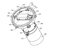
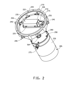
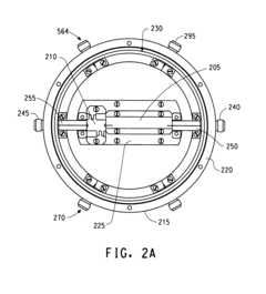
A thermalization arrangement at cryogenic temperatures
PatentWO2022180302A1
Innovation
- A thermalization arrangement with a dielectric substrate and a conductive layer between the substrate and heat sink, where phonons are absorbed by electrons, minimizing thermal boundary resistance and enhancing energy transfer through a conductive joint to an efficient heat sink component, thereby eliminating phonon reflections and improving cooling efficiency.
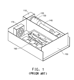
Cryogenic devices
PatentInactiveUS6688127B2
Innovation
- A cryogenic front-end unit with a cryogenic electronic portion within a vacuum dewar assembly, utilizing high-temperature superconductor filters and low-dissipated power semiconductor circuits, along with thermal break interconnects to reduce thermal transmission and power consumption, allowing for miniaturization and integration with reduced cooling requirements.
Materials Science Advancements for Cryogenic Applications
The evolution of cryogenic electronics has been significantly influenced by advancements in materials science. Traditional conducting materials often exhibit altered properties at extremely low temperatures, necessitating specialized materials engineered specifically for cryogenic environments. Recent breakthroughs in superconducting materials have enabled quantum computing applications with substantially reduced thermal noise profiles, particularly materials achieving superconductivity above 20K.
Novel composite materials incorporating rare earth elements have demonstrated exceptional thermal stability and electrical conductivity at temperatures approaching absolute zero. These materials exhibit minimal thermal expansion coefficients and maintain consistent electrical properties across wide temperature gradients, critical for maintaining signal integrity in sensitive cryogenic circuits. Research indicates that nanostructured materials with engineered grain boundaries show particular promise in mitigating electron scattering effects that contribute to thermal noise.
Insulating materials have also undergone significant development, with aerogel-based substrates providing superior thermal isolation properties while maintaining structural integrity under extreme temperature cycling. These advanced insulators effectively compartmentalize critical circuit components, preventing thermal crosstalk between elements operating at different temperature regimes within the same system.
Packaging materials represent another crucial advancement area, with hermetically sealed ceramic-metal composites demonstrating exceptional performance in maintaining vacuum integrity and thermal isolation. These packaging solutions incorporate specialized thermal interface materials that accommodate the differential contraction rates between components while maintaining optimal thermal conductivity paths for controlled heat dissipation.
Thin-film deposition techniques have evolved to create ultra-pure material layers with precisely controlled thicknesses down to atomic scales. These techniques enable the fabrication of superconducting quantum interference devices (SQUIDs) and other sensitive components with minimal defect densities, directly correlating to reduced thermal noise floors in measurement applications.
Carbon-based materials, particularly graphene and carbon nanotubes, have emerged as promising candidates for cryogenic interconnects due to their unique ballistic electron transport properties at low temperatures. These materials demonstrate quantum conductance effects that remain stable across temperature fluctuations, providing more reliable signal transmission than conventional metal interconnects in cryogenic environments.
The integration of these advanced materials into practical cryogenic electronic systems requires sophisticated modeling and simulation tools that accurately predict material behavior at quantum scales. Computational materials science has thus become an essential complement to experimental approaches, accelerating the discovery and optimization of novel materials specifically engineered to minimize thermal noise in next-generation cryogenic electronic applications.
Quantum Computing Integration Opportunities
The integration of cryogenic electronics with quantum computing systems represents one of the most promising frontiers for both technologies. Quantum computers fundamentally require ultra-low temperatures to maintain quantum coherence, typically operating at millikelvin ranges. This creates a natural synergy with cryogenic electronics, which can provide the necessary control and readout circuitry while minimizing thermal noise introduction to the quantum system.
Several major quantum computing architectures stand to benefit significantly from advances in cryogenic electronics. Superconducting qubit systems, currently employed by industry leaders like IBM, Google, and Rigetti, require sophisticated control electronics that traditionally operate at room temperature, necessitating complex wiring solutions that introduce heat loads and signal degradation. By migrating control electronics to cryogenic temperatures, these systems could achieve higher fidelity operations and improved scalability.
Silicon-based quantum dot qubits present another compelling integration opportunity. These systems benefit from compatibility with existing semiconductor manufacturing processes while requiring cryogenic operating environments. The development of co-located cryogenic control electronics could dramatically reduce interconnect complexity and improve signal integrity, potentially accelerating the path to practical quantum advantage.
Trapped ion quantum computers, while operating at less extreme temperatures than superconducting systems, would also benefit from cryogenic electronics integration. The precision voltage control required for ion trapping and manipulation could be significantly enhanced through reduced thermal noise in the control circuitry, potentially improving coherence times and gate fidelities.
Beyond the direct control of quantum bits, cryogenic electronics offers opportunities for enhancing quantum error correction circuits. As quantum systems scale, error correction becomes increasingly critical, requiring fast, low-latency classical processing near the quantum processor. Cryogenic CMOS and superconducting digital logic could enable these error correction circuits to operate with minimal latency and heat generation.
The roadmap for integration appears to be progressing through several phases: first, moving analog control components to cryogenic environments; second, developing cryogenic digital processing capabilities; and ultimately creating fully integrated quantum-classical systems with sophisticated cryogenic control architectures. Companies like Intel, IBM, and Microsoft are actively pursuing research in this direction, recognizing the potential competitive advantage of mastering this integration challenge.
Unlock deeper insights with Patsnap Eureka Quick Research — get a full tech report to explore trends and direct your research. Try now!
Generate Your Research Report Instantly with AI Agent
Supercharge your innovation with Patsnap Eureka AI Agent Platform!