

Cryogenic Electronics Patents: A Landscape Overview
SEP 29, 20259 MIN READ
Generate Your Research Report Instantly with AI Agent
Patsnap Eureka helps you evaluate technical feasibility & market potential.
Cryogenic Electronics Evolution and Research Objectives
Cryogenic electronics represents a specialized field at the intersection of quantum physics, materials science, and electronic engineering, focusing on the behavior and application of electronic systems at extremely low temperatures. The evolution of this field traces back to the early 20th century with the discovery of superconductivity by Heike Kamerlingh Onnes in 1911, marking the beginning of scientific interest in low-temperature electronic phenomena.
The 1950s and 1960s witnessed significant advancements with the development of theoretical frameworks explaining superconductivity, notably the BCS theory by Bardeen, Cooper, and Schrieffer in 1957. This period also saw the emergence of practical applications, including the first superconducting computing elements and memory devices, establishing the foundation for modern cryogenic electronics.
The 1980s brought revolutionary progress with the discovery of high-temperature superconductors, which operate at temperatures achievable with liquid nitrogen rather than the more expensive liquid helium. This breakthrough substantially reduced operational costs and expanded potential applications, catalyzing increased research interest and patent activity in the field.
Recent decades have seen accelerated development driven by quantum computing requirements, with companies like IBM, Google, and D-Wave Systems heavily investing in cryogenic electronic systems to support their quantum processors. The patent landscape reflects this trend, showing significant growth in filings related to superconducting quantum bits (qubits), cryogenic memory systems, and ultra-low-temperature control electronics.
The primary research objectives in cryogenic electronics currently focus on several key areas. First, developing more energy-efficient cooling systems to make cryogenic electronics commercially viable beyond specialized applications. Second, creating robust interface technologies between room-temperature and cryogenic components to enable practical system integration. Third, advancing materials science to discover new superconducting materials with improved properties at higher temperatures.
Additionally, researchers aim to miniaturize cryogenic electronic components for integration into more compact systems, particularly for space applications where size and weight constraints are critical. There is also significant interest in developing standardized design methodologies and testing protocols specifically for cryogenic electronic systems, addressing the unique challenges of low-temperature operation.
The patent landscape analysis reveals concentrated research efforts in quantum computing applications, space technology, medical imaging systems (particularly MRI technology), and ultra-sensitive detection systems. These areas represent the most promising commercial applications driving innovation in cryogenic electronics, with corresponding patent activity reflecting strategic positioning by industry leaders and research institutions.
Market Analysis for Cryogenic Electronic Applications
The cryogenic electronics market is experiencing significant growth driven by advancements in quantum computing, superconducting technologies, and space exploration. Current market estimates value the global cryogenic electronics sector at approximately $4.2 billion, with projections indicating a compound annual growth rate of 7.8% through 2028. This growth trajectory is primarily fueled by increasing investments in quantum computing research and development, which requires ultra-low temperature operating environments to maintain quantum coherence.
The quantum computing segment represents the largest application area for cryogenic electronics, accounting for nearly 42% of the total market share. Major technology companies including IBM, Google, and Intel have substantially increased their investments in quantum computing hardware that operates at temperatures approaching absolute zero. These investments are expected to drive the demand for specialized cryogenic electronic components including superconducting qubits, cryogenic amplifiers, and control systems.
Medical imaging applications, particularly in Magnetic Resonance Imaging (MRI) systems, constitute the second-largest market segment at 28%. The need for superconducting magnets in these systems creates consistent demand for cryogenic electronic components that can function reliably at liquid helium temperatures. The healthcare sector's expansion in emerging economies is further accelerating this demand.
Space exploration and satellite communications represent a rapidly growing application segment, currently at 15% of the market but expected to reach 22% by 2027. The extreme temperature conditions of space necessitate electronics that can function reliably in cryogenic environments. NASA, ESA, and private space companies are increasingly incorporating cryogenic electronics in deep space missions and satellite systems.
Regional analysis shows North America leading the market with 38% share, followed by Europe (29%) and Asia-Pacific (24%). China's accelerated investments in quantum technologies are expected to significantly alter this distribution over the next five years, potentially increasing Asia-Pacific's share to 32%.
The market faces several challenges, including high production costs, limited manufacturing capabilities for specialized components, and the need for extensive testing under extreme conditions. The average development cycle for new cryogenic electronic components remains lengthy at 18-24 months, creating barriers to rapid market expansion.
Despite these challenges, the increasing patent activity in cryogenic electronics indicates strong market potential. Patent filings have grown by 34% over the past three years, with superconducting circuit designs and cryogenic memory systems showing the highest growth rates. This patent landscape suggests that market participants anticipate substantial commercial applications emerging from current research efforts.
Global Cryogenic Electronics Development Status and Barriers
The global landscape of cryogenic electronics exhibits significant disparities in development across different regions. The United States maintains a dominant position, with substantial investments from both government agencies like DARPA and NASA, and private corporations such as IBM and Google. These entities focus primarily on quantum computing applications and superconducting electronics. The US advantage stems from decades of consistent funding and established research infrastructure at institutions like MIT, Stanford, and national laboratories.
Europe follows as the second major hub, with particularly strong contributions from Germany, France, and the Netherlands. The European Union's Quantum Flagship program has allocated over €1 billion for quantum technologies, with a significant portion directed toward cryogenic electronics development. European research excels in superconducting sensors and detectors, with organizations like CERN driving innovation in this space.
Japan and South Korea represent significant players in Asia, with Japan's historical strength in superconductivity research and Korea's growing investments in quantum technologies. China has rapidly accelerated its efforts in recent years, establishing dedicated research centers and increasing patent filings in cryogenic electronics, particularly for quantum computing applications.
Despite global progress, several critical barriers impede broader implementation of cryogenic electronics. The most fundamental challenge remains cooling technology limitations. Current cryogenic systems are bulky, energy-intensive, and expensive to operate, requiring specialized infrastructure and expertise. The cost of liquid helium, the primary coolant for ultra-low temperature applications, continues to rise due to global supply constraints.
Material science presents another significant hurdle. Developing materials that maintain desirable electronic properties at cryogenic temperatures while offering manufacturing compatibility with existing semiconductor processes remains challenging. Interface issues between room-temperature and cryogenic components create signal integrity problems and thermal management complications.
Standardization represents a critical barrier to commercialization. The lack of unified testing protocols, performance metrics, and interface standards hampers interoperability and slows industry adoption. Additionally, the specialized knowledge required for cryogenic electronics design creates a talent bottleneck, with few educational programs specifically addressing this interdisciplinary field.
Manufacturing scalability presents perhaps the most significant obstacle to widespread adoption. Current fabrication techniques for cryogenic electronics remain largely experimental or small-scale, with limited compatibility with high-volume semiconductor manufacturing processes. This creates substantial challenges for cost reduction and commercial viability beyond specialized applications.
Current Cryogenic Electronics Patent Solutions
01 Cryogenic cooling systems for electronic components
Specialized cooling systems designed to maintain electronic components at cryogenic temperatures for optimal performance. These systems utilize various refrigeration techniques to achieve and maintain extremely low temperatures required for superconducting electronics and quantum computing applications. The cooling infrastructure includes circulation systems, thermal interfaces, and insulation to ensure stable operation while minimizing thermal losses.- Superconducting electronic devices: Cryogenic electronics leverages superconducting materials that exhibit zero electrical resistance at extremely low temperatures. These devices include superconducting quantum interference devices (SQUIDs), Josephson junctions, and other quantum computing components that operate at temperatures near absolute zero. The superconducting state enables ultra-high-speed processing, reduced power consumption, and enhanced sensitivity for sensing applications, making them ideal for quantum computing and precision measurements.
- Cryogenic cooling systems for electronics: Specialized cooling systems are essential for maintaining the extremely low temperatures required for cryogenic electronics. These systems employ various refrigeration techniques including liquid helium, liquid nitrogen, pulse tube coolers, and Stirling cycle refrigerators. Advanced thermal management solutions ensure stable operating temperatures while minimizing thermal interference. These cooling infrastructures are critical for maintaining superconducting states and ensuring reliable operation of cryogenic electronic components.
- Cryogenic electronic packaging and interconnects: Specialized packaging solutions are designed to protect and connect cryogenic electronic components while maintaining thermal isolation from the ambient environment. These include vacuum-insulated enclosures, specialized circuit boards, and thermal isolation techniques. Cryogenic interconnects must address challenges such as thermal contraction, material compatibility, and signal integrity at extremely low temperatures. Advanced materials and designs ensure reliable electrical connections while minimizing heat transfer to the cold electronics.
- Cryogenic computing architectures: Computing systems designed specifically for operation at cryogenic temperatures leverage the unique properties of superconducting materials to achieve superior performance. These architectures include specialized logic gates, memory elements, and data processing units optimized for ultra-low temperature operation. Cryogenic computing offers advantages such as reduced power consumption, increased processing speed, and enhanced quantum coherence, making it particularly valuable for applications in quantum computing, space exploration, and high-performance computing.
- Cryogenic sensors and instrumentation: Sensors and measurement instruments designed to operate at cryogenic temperatures provide exceptional sensitivity and precision. These include magnetic field sensors, radiation detectors, and various scientific instruments that leverage the unique properties of materials at extremely low temperatures. Cryogenic sensors offer improved signal-to-noise ratios, enhanced detection capabilities, and greater measurement accuracy compared to room-temperature alternatives, making them essential for scientific research, medical imaging, and advanced industrial applications.
02 Superconducting electronic circuits and devices
Electronic circuits and devices designed to operate at cryogenic temperatures to leverage superconductivity properties. These include superconducting processors, memory elements, and interconnects that exhibit zero electrical resistance at extremely low temperatures. The designs incorporate specialized materials and architectures optimized for quantum coherence and reduced thermal noise, enabling higher processing speeds and energy efficiency compared to conventional electronics.Expand Specific Solutions03 Thermal management and packaging for cryogenic electronics
Advanced packaging solutions and thermal management techniques specifically designed for electronics operating at cryogenic temperatures. These include specialized materials with matched thermal expansion coefficients, thermal interfaces that maintain conductivity at low temperatures, and multi-layer insulation systems. The packaging must address challenges such as thermal cycling, mechanical stress, and electrical interconnection while maintaining the required operating temperature for the electronic components.Expand Specific Solutions04 Quantum computing hardware and cryogenic control systems
Hardware architectures and control systems designed specifically for quantum computing applications operating at cryogenic temperatures. These systems include qubit arrays, control electronics, readout circuits, and signal processing components that must function reliably at extremely low temperatures. The designs address challenges such as quantum coherence preservation, signal integrity, and the integration of classical control electronics with quantum processing elements.Expand Specific Solutions05 Cryogenic electronic testing and measurement equipment
Specialized equipment and methodologies for testing and characterizing electronic components and systems at cryogenic temperatures. These include cryostats with integrated measurement capabilities, low-temperature probe stations, and calibrated instrumentation systems designed to operate in extreme cold. The equipment enables accurate performance evaluation, reliability testing, and failure analysis of components intended for cryogenic applications while maintaining precise temperature control throughout the testing process.Expand Specific Solutions
Leading Organizations in Cryogenic Electronics Patent Landscape
Cryogenic electronics is currently in an early growth phase, with the market expanding due to quantum computing and superconducting applications. The global market size remains relatively niche but is projected to grow significantly as quantum technologies mature. Technologically, IBM leads the field with substantial patent holdings, followed by Microsoft Technology Licensing and Northrop Grumman Systems in developing superconducting circuits and quantum processors. Other key players include Google, PsiQuantum, and Quantinuum, focusing on quantum computing applications, while specialized firms like Montana Instruments and Synergy Systems Corporation provide essential cryogenic support systems. Research institutions such as Naval Research Laboratory and Max Planck Society contribute fundamental breakthroughs, indicating a blend of established corporations and specialized innovators driving advancement in this emerging field.
International Business Machines Corp.
Technical Solution: IBM has pioneered significant advancements in cryogenic electronics, particularly focusing on superconducting quantum computing systems. Their technology involves developing Josephson junction-based superconducting qubits that operate at temperatures near absolute zero (typically below 20 millikelvin). IBM's cryogenic electronics patents cover specialized control systems, including cryogenic CMOS circuits designed to function at extremely low temperatures, reducing the thermal load on dilution refrigerators. They've developed proprietary techniques for quantum-classical interface electronics that can operate in close proximity to quantum processors, minimizing signal latency and decoherence effects. IBM has also patented specialized packaging solutions that address thermal isolation challenges and enable efficient signal transmission between room temperature control systems and cryogenic quantum processors[1][3]. Their cryogenic multiplexing technology allows for controlling thousands of qubits with minimal external connections, which is crucial for scaling quantum systems.
Strengths: IBM possesses extensive intellectual property in cryogenic control electronics that enables practical quantum computing implementations. Their integrated approach combining hardware and software gives them a competitive advantage in system-level solutions. Weaknesses: The extreme cooling requirements create significant engineering challenges for widespread deployment, and the specialized manufacturing processes for cryogenic components limit production scaling and increase costs.
Northrop Grumman Systems Corp.
Technical Solution: Northrop Grumman has developed extensive cryogenic electronics technology focused on superconducting digital and RF systems. Their patents cover Superconducting Single Flux Quantum (SFQ) logic circuits that leverage the unique properties of superconductors to create ultra-high-speed, low-power digital systems operating at liquid helium temperatures (4K). The company has pioneered Reciprocal Quantum Logic (RQL) technology, a variant of SFQ that offers improved energy efficiency and simpler circuit implementation. Northrop's cryogenic electronics portfolio includes specialized cryogenic memory systems based on Josephson junctions that can interface with superconducting processors without energy-intensive temperature transitions[2]. They've also patented cryogenic RF components including filters, amplifiers, and mixers that demonstrate exceptional performance metrics impossible at room temperature. Their integrated cryopackaging solutions address the challenges of connecting room-temperature systems to cryogenic circuits while minimizing thermal loading and maintaining signal integrity across extreme temperature gradients[5].
Strengths: Northrop Grumman's technologies offer unparalleled speed and energy efficiency for specialized computing and signal processing applications, with demonstrated clock speeds in the hundreds of gigahertz range. Their defense industry focus has enabled sustained R&D investment in this specialized field. Weaknesses: The technologies require sophisticated cryogenic infrastructure, limiting deployment scenarios, and the specialized fabrication processes for superconducting circuits present manufacturing scalability challenges compared to conventional semiconductor approaches.
Critical Patent Analysis and Technical Innovations
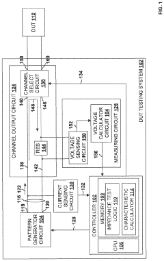
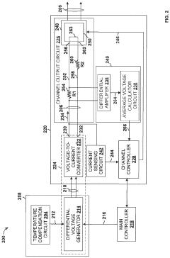
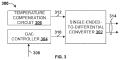
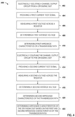
Systems and methods for measuring characteristics of cryogenic electronic devices
PatentActiveUS20230393182A1
Innovation
- A system and method that utilize a channel select circuit and a controller to electrically isolate and couple a channel output circuit to a cryogenic device under test, using test current signals to determine impedance characteristics by measuring voltages across resistors in the transmission path, thereby compensating for transmission path nonidealities and impedance mismatches.
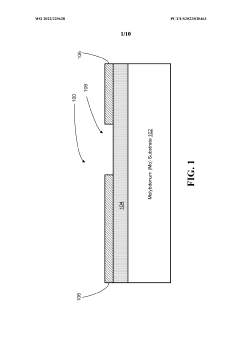
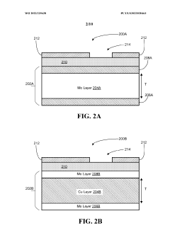
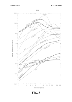
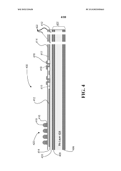
Multilayer superconducting structures for cryogenic electronics
PatentWO2022225628A1
Innovation
- The use of a molybdenum substrate with copper cladding layers, matched to the CTE of cryogenic electronic chips, provides improved thermal conductivity and reduced mechanical stresses, ensuring reliable operation from room temperature to deep cryogenic temperatures by fine-tuning the CTE and thermal conductivity characteristics through layer thickness and purity adjustments.
Patent Strategy and IP Protection in Cryogenic Electronics
In the rapidly evolving field of cryogenic electronics, patent strategy and intellectual property protection have become critical components for companies seeking competitive advantage. The patent landscape reveals a complex web of IP rights concentrated among a few major players, with IBM, Intel, and D-Wave Systems holding significant patent portfolios. These companies have adopted different strategies, with IBM focusing on broad foundational patents covering superconducting materials and circuit designs, while Intel emphasizes integration technologies between cryogenic and conventional electronics.
Strategic patent filing patterns indicate geographical preferences, with the United States Patent and Trademark Office (USPTO) receiving the highest number of cryogenic electronics patent applications, followed by the European Patent Office (EPO) and China's National Intellectual Property Administration (CNIPA). This distribution reflects the global research centers and market priorities in this specialized field.
Protection strategies commonly employed include building patent thickets around core technologies, particularly for quantum computing applications where cryogenic electronics serve as enabling technologies. Companies are increasingly filing continuation patents to extend protection periods and adapt claims as the technology evolves, creating multi-layered IP barriers against competitors.
Cross-licensing agreements have emerged as a practical solution in this technologically interdependent field, with major players establishing strategic partnerships to navigate the complex patent landscape. Notable examples include collaborations between quantum computing companies and cryogenic cooling system manufacturers, where complementary IP portfolios create mutually beneficial arrangements.
Emerging IP challenges include determining patentability boundaries for quantum-classical interfaces and addressing the increasing overlap between academic research and commercial applications. Universities and research institutions hold approximately 30% of cryogenic electronics patents, creating a dynamic ecosystem where knowledge transfer and IP licensing play crucial roles.
For companies entering this space, recommended IP strategies include focused patent filing in specific application areas rather than attempting to compete with established players on fundamental technologies. Defensive publication strategies are also gaining traction, particularly for incremental innovations that may not warrant full patent protection but serve to prevent competitors from obtaining exclusive rights.
The future IP landscape will likely see increased patent activity in cryogenic memory technologies, superconducting interconnects, and energy-efficient cryogenic control systems, reflecting the industry's push toward practical quantum computing implementations and ultra-low-power electronics applications.
Quantum Computing Integration with Cryogenic Electronics
The integration of quantum computing with cryogenic electronics represents a critical frontier in advancing quantum technologies. Quantum computers require ultra-low temperatures to maintain quantum coherence, typically operating below 100 millikelvin. This necessity has created a symbiotic relationship between quantum computing development and cryogenic electronics innovation, as evidenced in patent landscapes across both domains.
Recent patent analyses reveal significant growth in technologies bridging these fields, with major filings concentrated on superconducting quantum circuits that can operate at cryogenic temperatures. IBM, Google, Intel, and D-Wave Systems have emerged as leading patent holders, focusing on scalable architectures that integrate quantum processing units with cryogenic control electronics.
A notable trend in patent filings involves the development of cryogenic CMOS technologies specifically designed to function at quantum-relevant temperatures. These innovations aim to place classical control electronics in closer proximity to quantum bits, reducing latency and signal degradation while managing thermal loads - a persistent challenge in quantum system design.
Superconducting interconnect technologies represent another active area of patent development, with innovations focusing on efficient signal transmission between room temperature systems and quantum processors. Materials science breakthroughs, particularly regarding superconducting materials with higher critical temperatures, feature prominently in recent patent applications.
The patent landscape also reflects growing interest in cryogenic memory solutions compatible with quantum computing architectures. These developments address the need for ultra-low power, high-density memory systems that can operate reliably in extreme cold environments without introducing thermal noise to quantum circuits.
Intellectual property related to thermal management systems shows increasing sophistication, with patents covering multi-stage cooling architectures and novel refrigeration cycles designed specifically for quantum computing applications. These innovations aim to balance the competing demands of cooling capacity, energy efficiency, and system reliability.
Cross-licensing agreements between quantum computing companies and cryogenic electronics specialists have accelerated in recent years, indicating a recognition that expertise from both domains is essential for commercial viability. This collaborative approach is reflected in joint patent applications that span traditional technology boundaries.
Unlock deeper insights with Patsnap Eureka Quick Research — get a full tech report to explore trends and direct your research. Try now!
Generate Your Research Report Instantly with AI Agent
Supercharge your innovation with Patsnap Eureka AI Agent Platform!