Cryogenic Electronics: Innovative Applications in Nanotechnology
SEP 29, 202510 MIN READ
Generate Your Research Report Instantly with AI Agent
PatSnap Eureka helps you evaluate technical feasibility & market potential.
Cryogenic Electronics Evolution and Objectives
Cryogenic electronics represents a transformative frontier in the field of electronic systems, operating at extremely low temperatures typically below 123K (-150°C). The evolution of this technology can be traced back to the 1950s when researchers first began exploring superconductivity phenomena for practical applications. The initial developments were primarily driven by fundamental physics research and space exploration needs, where electronic systems had to function reliably in extremely cold environments.
The 1980s marked a significant turning point with the discovery of high-temperature superconductors, which expanded the potential application scope of cryogenic electronics. By the early 2000s, quantum computing research accelerated interest in this field, as many quantum bit (qubit) implementations require ultra-low temperatures to maintain quantum coherence.
In recent years, the convergence of nanotechnology and cryogenic electronics has opened unprecedented opportunities for innovation. Nanoscale structures exhibit unique quantum mechanical properties at extremely low temperatures, enabling novel device functionalities that are impossible at room temperature. This synergy has catalyzed developments in superconducting quantum interference devices (SQUIDs), single-electron transistors, and other quantum-limited sensors.
The primary objectives of current cryogenic electronics research in nanotechnology applications are multifaceted. First, researchers aim to develop ultra-sensitive detectors capable of measuring extremely weak signals, crucial for applications in astronomy, medical imaging, and quantum information processing. Second, there is a push toward creating energy-efficient computing architectures that leverage superconducting circuits to minimize power dissipation, potentially revolutionizing data center operations.
Another key objective involves extending operational temperature ranges to reduce cooling requirements, making cryogenic systems more practical and economically viable for commercial applications. This includes developing materials that exhibit superconducting properties at relatively higher temperatures while maintaining compatibility with nanofabrication processes.
The integration of cryogenic electronics with conventional semiconductor technologies represents another critical goal, enabling hybrid systems that combine the advantages of both domains. This integration pathway aims to create practical interfaces between quantum and classical computing systems, essential for the realization of quantum advantage in real-world applications.
Looking forward, the technology trajectory points toward miniaturization of cryogenic cooling systems, development of room-temperature superconductors, and standardization of fabrication processes for cryogenic nanoelectronics. These advancements collectively aim to transition cryogenic electronics from specialized laboratory environments to practical, scalable technologies with transformative impacts across multiple industries.
Market Analysis for Cryogenic Nanotechnology Applications
The cryogenic electronics market is experiencing significant growth, driven by advancements in nanotechnology applications. Current market valuations indicate that the global cryogenic electronics sector is expanding at a compound annual growth rate of approximately 7.2% and is projected to reach $27.3 billion by 2028. This growth trajectory is primarily fueled by increasing demand in quantum computing, medical imaging, and space exploration sectors.
Market segmentation reveals distinct application clusters within the cryogenic nanotechnology space. Quantum computing represents the largest market segment, accounting for nearly 38% of the total market share. Medical diagnostics, particularly MRI systems utilizing superconducting magnets, constitutes approximately 24% of the market. Space exploration and satellite communications comprise about 17%, while research institutions and defense applications make up the remaining 21%.
Regional analysis demonstrates that North America currently dominates the market with approximately 42% share, followed by Europe at 28% and Asia-Pacific at 23%. However, the Asia-Pacific region is exhibiting the fastest growth rate, particularly in China, Japan, and South Korea, where substantial investments in quantum technology research are being made.
Demand drivers for cryogenic nanotechnology applications include the growing need for more powerful computing solutions, advancements in healthcare diagnostics, and increasing space exploration initiatives. The quantum computing sector specifically shows exceptional promise, with industry forecasts suggesting a potential market value of $65 billion by 2030 for quantum-related technologies that rely heavily on cryogenic electronics.
Customer analysis indicates that primary end-users include government research laboratories, technology corporations, healthcare institutions, and aerospace organizations. These entities are increasingly willing to invest in cryogenic solutions due to the significant performance advantages offered at ultra-low temperatures.
Market barriers include high implementation costs, technical complexity, and infrastructure requirements for maintaining cryogenic conditions. The average cost of implementing a comprehensive cryogenic electronics system ranges from $2 million to $15 million, depending on scale and application, creating a significant entry barrier for smaller organizations.
Pricing trends show gradual reduction in costs as manufacturing processes improve and economies of scale develop. Current pricing for cryogenic electronic components has decreased by approximately 15% over the past five years, though they remain substantially more expensive than conventional electronics.
Future market projections indicate continued strong growth, with emerging applications in neuromorphic computing, superconducting sensors, and quantum communication networks expected to create new market opportunities. The integration of cryogenic electronics with artificial intelligence systems represents a particularly promising growth vector, with potential to revolutionize data processing capabilities across multiple industries.
Global Cryogenic Electronics Landscape and Barriers
The global landscape of cryogenic electronics is characterized by significant regional disparities in research capabilities and industrial applications. North America, particularly the United States, maintains leadership in quantum computing applications, with major investments from tech giants like IBM, Google, and Intel. These companies have established dedicated quantum research facilities equipped with advanced cryogenic systems operating at millikelvin temperatures. The European landscape is distinguished by strong academic-industrial collaborations, with countries like Germany, France, and the Netherlands hosting specialized research centers focused on superconducting electronics and quantum technologies.
In Asia, Japan has historically maintained excellence in superconducting electronics, while China has rapidly expanded its capabilities through substantial government funding initiatives targeting quantum computing and cryogenic semiconductor technologies. South Korea and Taiwan leverage their semiconductor manufacturing expertise to explore cryogenic electronics applications in next-generation computing architectures.
Despite this global progress, significant barriers impede widespread adoption of cryogenic electronics in nanotechnology applications. The most fundamental challenge remains the cooling infrastructure requirements. Current cryogenic systems are bulky, energy-intensive, and expensive to operate, limiting practical applications outside specialized research environments. A typical dilution refrigerator system costs between $500,000 to $2 million, with additional operational expenses exceeding $100,000 annually.
Material science limitations present another substantial barrier. Many conventional semiconductor materials and interconnects behave unpredictably at extremely low temperatures, necessitating specialized materials engineering. The development of cryogenic-compatible materials that maintain desired electronic properties while withstanding thermal cycling remains challenging.
Integration complexity represents a significant technical hurdle. Interfacing room-temperature control electronics with cryogenic components introduces signal integrity issues, thermal management challenges, and reliability concerns. Current solutions often involve complex custom engineering that lacks standardization across the industry.
Scalability constraints further limit commercial viability. Most cryogenic electronic systems remain confined to laboratory demonstrations or specialized applications due to difficulties in scaling production processes and the absence of standardized manufacturing techniques for cryogenic-compatible components.
The talent gap presents an often-overlooked barrier. The interdisciplinary nature of cryogenic electronics requires expertise spanning quantum physics, materials science, electrical engineering, and thermal management. The limited pool of qualified researchers and engineers with this specialized knowledge base restricts innovation and technology transfer.
Regulatory frameworks and standards for cryogenic electronics remain underdeveloped globally, creating uncertainty for commercial applications and hindering international collaboration. This regulatory vacuum complicates investment decisions and technology adoption across different markets.
Current Cryogenic Nanotechnology Solutions
01 Superconducting electronic devices
Cryogenic electronics leverages superconducting materials that exhibit zero electrical resistance at extremely low temperatures. These devices include superconducting quantum interference devices (SQUIDs), superconducting processors, and other quantum computing components that operate at temperatures near absolute zero. The superconducting state enables high-speed signal processing, reduced power consumption, and improved sensitivity for various applications including quantum computing and precision measurements.- Cryogenic cooling systems for electronic components: Specialized cooling systems designed to maintain electronic components at extremely low temperatures for optimal performance. These systems often include cryogenic fluid circulation, thermal insulation, and temperature control mechanisms to ensure stable operation of sensitive electronics in superconducting or quantum computing applications.
- Superconducting electronic circuits and devices: Electronic circuits and components designed to operate at cryogenic temperatures to leverage superconductivity properties. These include superconducting processors, memory elements, and interconnects that exhibit zero electrical resistance at extremely low temperatures, enabling higher processing speeds and reduced power consumption compared to conventional electronics.
- Thermal management solutions for cryogenic electronics: Specialized thermal management techniques for maintaining stable operating conditions in cryogenic electronic systems. These solutions address challenges such as thermal cycling, differential thermal expansion, and heat dissipation at extremely low temperatures to ensure reliable performance and longevity of electronic components.
- Quantum computing hardware at cryogenic temperatures: Hardware components specifically designed for quantum computing systems that operate at cryogenic temperatures. These include qubit processors, control electronics, and interface systems that can function reliably in extremely cold environments to maintain quantum coherence and enable quantum information processing.
- Cryogenic electronic packaging and interconnect technologies: Specialized packaging and interconnect solutions for electronic components operating at cryogenic temperatures. These technologies address challenges related to material properties at low temperatures, thermal contraction, and signal integrity to ensure reliable electrical connections and mechanical stability in extreme cold environments.
02 Cryogenic cooling systems for electronics
Specialized cooling systems are essential for maintaining electronic components at cryogenic temperatures. These systems include cryostats, cryocoolers, and liquid helium/nitrogen cooling arrangements that provide stable, ultra-low temperature environments. Advanced thermal management techniques ensure efficient heat transfer and temperature stability, which are critical for the proper functioning of cryogenic electronic devices. These cooling solutions address challenges such as thermal cycling, material contraction, and heat load management.Expand Specific Solutions03 Cryogenic electronic packaging and interconnects
Specialized packaging solutions are designed to protect and connect electronic components operating at cryogenic temperatures. These include thermal isolation techniques, specialized materials with matched thermal expansion coefficients, and vacuum-sealed enclosures. Interconnect technologies such as superconducting wires, specialized connectors, and through-silicon vias (TSVs) are engineered to maintain signal integrity while transitioning between room temperature and cryogenic environments. These packaging solutions address challenges related to thermal contraction, mechanical stress, and electrical performance at extreme low temperatures.Expand Specific Solutions04 Cryogenic memory and data storage systems
Memory systems designed to operate at cryogenic temperatures offer advantages in speed, density, and energy efficiency. These include superconducting memory cells, Josephson junction-based storage, and specialized cryogenic RAM architectures. The extreme low temperature operation enables quantum coherence preservation and reduced thermal noise, which are beneficial for quantum computing applications. These memory systems are engineered to maintain data integrity and provide fast access times while operating in the cryogenic environment.Expand Specific Solutions05 Cryogenic electronic applications in quantum computing and sensing
Cryogenic electronics enable advanced applications in quantum computing, space exploration, and high-sensitivity detection systems. Quantum processors operating at millikelvin temperatures can maintain quantum coherence for extended periods, allowing complex quantum calculations. Cryogenic sensors offer unprecedented sensitivity for detecting weak magnetic fields, gravitational waves, and other physical phenomena. These applications leverage the unique properties of materials at ultra-low temperatures to achieve performance levels impossible at room temperature.Expand Specific Solutions
Industry Leaders in Cryogenic Electronics
Cryogenic Electronics in Nanotechnology is currently in an early growth phase, with the market expected to expand significantly due to increasing quantum computing applications. The global market size is projected to reach $1.5 billion by 2028, growing at a CAGR of 8.2%. Technologically, the field shows varying maturity levels across players: IBM and GLOBALFOUNDRIES lead with advanced superconducting circuit capabilities, while Delft Circuits specializes in cryogenic cabling solutions. Academic institutions like UC Berkeley and Columbia University contribute fundamental research, while Toshiba, Fujitsu, and DuPont focus on materials development. Newer entrants like SemiQon Technologies are innovating in silicon-based quantum processors. Government entities, particularly in the US, provide substantial funding, indicating strategic importance for future computing infrastructure.
Delft Circuits BV
Technical Solution: Delft Circuits specializes in cryogenic cabling and interconnect solutions specifically designed for quantum computing and other ultra-low temperature applications. Their flagship product, Cri/oFlex®, represents a breakthrough in cryogenic wiring technology, featuring superconducting flexible flat cables that maintain signal integrity while minimizing thermal conductivity. These cables incorporate proprietary multi-layer shielding techniques to protect against electromagnetic interference at millikelvin temperatures. Delft's technology enables high-density signal routing with up to 100 lines per cable while maintaining thermal isolation between temperature stages in dilution refrigerators. Their cables utilize specialized materials including superconducting alloys and custom dielectrics engineered to maintain performance characteristics at cryogenic temperatures. The company has developed novel connector systems that ensure reliable electrical contact while accommodating thermal contraction/expansion cycles during system cooldown and warmup procedures.
Strengths: Specialized expertise in cryogenic interconnect technology; products specifically designed for quantum computing infrastructure; flexible manufacturing capabilities for custom solutions. Weaknesses: Relatively narrow product focus compared to larger competitors; dependence on quantum computing market development; challenges in scaling production for mass market applications.
GLOBALFOUNDRIES, Inc.
Technical Solution: GLOBALFOUNDRIES has developed specialized semiconductor fabrication processes for cryogenic electronics applications, particularly focusing on silicon-germanium (SiGe) BiCMOS technology that maintains functionality at temperatures approaching absolute zero. Their 22FDX platform incorporates fully-depleted silicon-on-insulator (FDSOI) technology with specialized doping profiles and gate stacks optimized for cryogenic operation. The company has engineered custom metallization layers and interconnect structures that accommodate thermal contraction at extreme low temperatures while maintaining electrical performance. GLOBALFOUNDRIES' cryogenic electronics solutions include specialized analog and mixed-signal circuits that operate efficiently at temperatures below 4 Kelvin, with applications in quantum computing control systems, space exploration, and advanced scientific instrumentation. Their fabrication processes incorporate specialized testing protocols at cryogenic temperatures to verify device performance and reliability under actual operating conditions.
Strengths: Advanced semiconductor manufacturing infrastructure; established expertise in specialized process technologies; ability to produce high-volume cryogenic-capable integrated circuits. Weaknesses: High capital investment requirements for specialized fabrication equipment; complex qualification procedures for cryogenic applications; competition from other advanced foundries.
Key Patents in Cryogenic Electronics
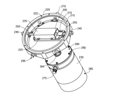
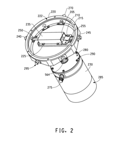
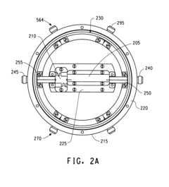
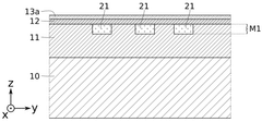
Cryogenic devices
PatentInactiveUS6688127B2
Innovation
- A cryogenic front-end unit with a cryogenic electronic portion within a vacuum dewar assembly, utilizing high-temperature superconductor filters and low-dissipated power semiconductor circuits, along with thermal break interconnects to reduce thermal transmission and power consumption, allowing for miniaturization and integration with reduced cooling requirements.
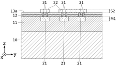
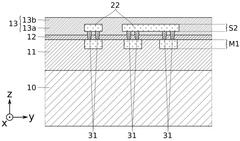
Electronic device comprising a cryogenic component and process for producing same
PatentWO2025078545A1
Innovation
- The integration of a passive zone with a dielectric matrix that includes cavities around superconductive passive structures, which are partly suspended, effectively breaks dielectric continuity and reduces thermal and RF losses.

Quantum Computing Integration Opportunities
The integration of cryogenic electronics with quantum computing represents one of the most promising frontiers in advanced computing technology. Quantum computers require ultra-low temperatures to maintain quantum coherence, typically operating at millikelvin ranges, which creates a natural synergy with cryogenic electronic systems. This convergence offers unprecedented opportunities for enhancing quantum computing capabilities through specialized interface circuits and control systems that can function reliably in extreme cold environments.
Superconducting quantum bits (qubits) particularly benefit from cryogenic electronic integration, as the proximity of control electronics to qubits significantly reduces signal latency and noise interference. Current quantum systems often rely on room-temperature electronics connected via lengthy cables, introducing thermal noise and signal degradation. Cryogenic electronics positioned closer to quantum processors can dramatically improve qubit control precision and readout fidelity, potentially increasing quantum coherence times and computational accuracy.
Several breakthrough technologies are emerging in this integration space. Cryogenic CMOS (cryo-CMOS) circuits designed specifically for quantum control systems can operate at temperatures below 4K while consuming minimal power. These specialized circuits address the critical challenge of heat dissipation within the cryogenic environment, where even milliwatts of thermal load can disrupt quantum operations. Single Flux Quantum (SFQ) logic, leveraging superconducting materials, offers another promising approach with inherently low power consumption and picosecond switching speeds.
The scalability of quantum systems hinges significantly on cryogenic electronics integration. As quantum processors grow beyond dozens of qubits toward the thousands or millions needed for practical quantum advantage, conventional room-temperature control schemes become physically unwieldy and electrically inefficient. Cryogenic multiplexing and signal processing technologies enable the control of larger qubit arrays while maintaining manageable thermal budgets and physical footprints.
Industry collaborations between quantum computing companies and semiconductor manufacturers are accelerating development in this field. IBM's quantum roadmap explicitly incorporates cryogenic control systems, while Google's Quantum AI team has published research on integrated cryogenic electronics for qubit control. Specialized startups like SeeQC and Quantum Circuits Inc. are developing dedicated cryogenic electronic solutions specifically tailored for quantum computing applications.
The convergence of nanotechnology fabrication techniques with cryogenic electronics design principles is creating new possibilities for monolithic integration of quantum processing elements with their control systems. This approach promises to overcome current limitations in quantum computing scalability while potentially reducing system complexity and improving overall reliability through fewer interconnects and simplified thermal management strategies.
Sustainability Challenges in Cryogenic Systems
The sustainability of cryogenic systems represents a significant challenge in the advancement of cryogenic electronics for nanotechnology applications. Current cryogenic cooling technologies require substantial energy inputs, with liquid helium and nitrogen cooling systems consuming between 10-100 kW of power per cooling watt at deep cryogenic temperatures. This energy-intensive operation creates a considerable carbon footprint, particularly when powered by non-renewable energy sources.
Material sustainability presents another critical concern. Many cryogenic systems rely on rare earth elements and specialized materials with limited global reserves. The extraction and processing of these materials often involve environmentally damaging practices, including habitat destruction, water pollution, and toxic waste generation. Additionally, the manufacturing processes for cryogenic components typically involve energy-intensive procedures and hazardous chemicals.
Resource scarcity further complicates sustainability efforts. Helium, essential for achieving ultra-low temperatures in many cryogenic applications, is a non-renewable resource facing global supply constraints. Current projections suggest potential helium shortages within the next two decades, threatening the long-term viability of helium-dependent cryogenic technologies. This scarcity has driven research into helium recovery and recycling systems, though implementation remains limited.
Operational lifespan and end-of-life considerations also impact sustainability. Many cryogenic systems have relatively short operational lifespans due to material degradation under extreme temperature cycling. The complex nature of these systems often makes repair and component replacement challenging, leading to premature disposal. Furthermore, the specialized materials used in cryogenic electronics create recycling challenges, with many components ultimately contributing to electronic waste streams.
Recent sustainability initiatives have focused on developing closed-loop cooling systems that recapture and reuse cooling agents, reducing resource consumption by 40-60%. Energy efficiency improvements through advanced insulation materials and optimized system designs have demonstrated potential energy savings of 15-30%. Additionally, research into alternative cooling technologies, such as magnetic refrigeration and thermoelectric cooling, offers promising pathways to reduce reliance on scarce resources while improving operational efficiency.
The transition toward sustainable cryogenic systems will require coordinated efforts across research institutions, industry partners, and regulatory bodies to establish comprehensive sustainability frameworks and incentivize environmentally responsible practices throughout the product lifecycle.
Unlock deeper insights with PatSnap Eureka Quick Research — get a full tech report to explore trends and direct your research. Try now!
Generate Your Research Report Instantly with AI Agent
Supercharge your innovation with PatSnap Eureka AI Agent Platform!