

DDR5 Integration with FPGA Designs for Optimized Performance
SEP 17, 20259 MIN READ
Generate Your Research Report Instantly with AI Agent
PatSnap Eureka helps you evaluate technical feasibility & market potential.
DDR5 Evolution and FPGA Integration Goals
DDR5 memory technology represents a significant evolution in the DRAM landscape, building upon its predecessor DDR4 with substantial improvements in bandwidth, capacity, and power efficiency. Since its introduction in 2021, DDR5 has established itself as the next-generation memory standard for high-performance computing applications. The technology offers data rates starting at 4800 MT/s and scaling up to 8400 MT/s in current implementations, with a roadmap extending to 12800 MT/s, effectively doubling the bandwidth capabilities of DDR4.
The historical progression from DDR4 to DDR5 marks a critical inflection point in memory architecture, introducing fundamental changes such as dual-channel architecture per DIMM, on-die ECC, and improved power management through voltage regulation moved from motherboards to the modules themselves. This evolution addresses the growing memory demands of data-intensive applications in artificial intelligence, machine learning, and high-performance computing sectors.
For FPGA designs, memory bandwidth has traditionally been a significant bottleneck limiting system performance. As FPGAs continue to increase in logic density and computational capabilities, the integration with high-speed memory subsystems becomes increasingly critical. The primary goal of DDR5 integration with FPGA designs is to eliminate this bottleneck by leveraging the enhanced bandwidth and reduced latency characteristics of DDR5 technology.
Technical objectives for this integration include achieving optimal signal integrity at higher frequencies, implementing efficient memory controllers capable of handling the increased complexity of DDR5 protocols, and developing power management strategies that capitalize on DDR5's improved energy efficiency features. Additionally, there is a focus on maximizing effective bandwidth utilization through advanced memory access patterns and scheduling algorithms specifically tailored to FPGA workloads.
The long-term technical trajectory aims to enable seamless scaling with future DDR5 speed grades while maintaining backward compatibility where possible. This includes developing flexible memory interface IP cores that can adapt to various DDR5 configurations and speed grades without requiring substantial redesign of the FPGA application logic.
Another critical goal is reducing the implementation complexity for end-users through abstracted memory interfaces and automated timing closure tools, allowing system designers to focus on their application logic rather than memory interface details. This democratization of high-performance memory access is essential for broadening the adoption of FPGA-based acceleration across diverse application domains.
Market Demand for High-Performance Memory in FPGA Systems
The demand for high-performance memory solutions in FPGA systems has experienced significant growth in recent years, driven by the increasing complexity of applications requiring enhanced data processing capabilities. As FPGAs continue to evolve from simple programmable logic devices to sophisticated system-on-chip solutions, the memory subsystem has become a critical factor in determining overall system performance.
Data-intensive applications such as artificial intelligence, machine learning, high-frequency trading, and real-time video processing have created substantial market pressure for memory systems that can deliver higher bandwidth, lower latency, and improved power efficiency. According to market research, the global FPGA market is projected to reach $15.5 billion by 2027, with memory integration solutions representing a significant growth segment within this market.
The transition from DDR4 to DDR5 memory technology represents a pivotal shift in addressing these market demands. Enterprise data centers, which constitute approximately 35% of the FPGA market, are particularly eager to adopt DDR5 integration solutions due to the exponential growth in data processing requirements and the need for improved server performance metrics.
Telecommunications infrastructure, another major consumer of FPGA technology, is experiencing increased demand for high-bandwidth memory solutions to support 5G network deployments. With data rates in 5G networks exceeding 10 Gbps, the memory subsystems in FPGA-based network equipment require significant upgrades to handle the increased throughput.
The automotive sector has emerged as a rapidly growing market for advanced FPGA memory solutions, particularly with the rise of autonomous driving technologies. These applications demand real-time processing of sensor data with extremely low latency, creating a market need for memory systems that can support parallel processing of multiple data streams simultaneously.
Cloud service providers have also become significant drivers of demand for high-performance FPGA memory solutions. As these providers increasingly deploy FPGAs as accelerators for specific workloads, the memory bandwidth has often become the limiting factor in achieving optimal performance. This has created a market opportunity for DDR5 integration solutions that can alleviate this bottleneck.
Market analysis indicates that customers are willing to pay a premium of 15-20% for FPGA solutions that incorporate DDR5 memory interfaces, compared to equivalent DDR4-based systems, reflecting the significant value placed on memory performance improvements in modern FPGA applications.
DDR5 Technical Challenges in FPGA Implementation
The integration of DDR5 memory with FPGA designs presents significant technical challenges that must be addressed to achieve optimal performance. The high-speed operation of DDR5, with data rates exceeding 4800 MT/s, creates signal integrity issues that are particularly problematic in FPGA implementations. These challenges are exacerbated by the limited I/O capabilities and fixed architecture of many FPGA platforms.
One primary challenge is the physical interface design. DDR5's stringent timing requirements demand precise signal routing and impedance matching. FPGAs, with their reconfigurable fabric, often struggle to maintain the tight timing margins required by DDR5 specifications. The differential signaling used in DDR5 requires careful consideration of trace lengths and impedance control, which can be difficult to achieve within the constraints of FPGA development boards.
Power management represents another significant hurdle. DDR5 operates at lower voltages (typically 1.1V) compared to previous generations, requiring more sophisticated power delivery networks. FPGAs must incorporate efficient voltage regulation modules to maintain stable power supply to DDR5 modules while managing the increased power density. The challenge is compounded by the need to minimize noise in the power distribution network, which can adversely affect signal integrity.
Protocol complexity introduces additional implementation difficulties. DDR5 incorporates advanced features such as Decision Feedback Equalization (DFE), on-die termination calibration, and enhanced refresh mechanisms. Implementing these features in FPGA logic consumes valuable resources and increases design complexity. The memory controller must handle these protocols efficiently while maintaining high throughput and low latency.
Thermal management presents a growing concern as DDR5 operates at higher frequencies and densities. The increased power consumption generates more heat, which must be effectively dissipated to prevent performance degradation. FPGA designs must incorporate thermal considerations into their layout and may require additional cooling solutions, particularly in space-constrained applications.
Testing and validation of DDR5 interfaces in FPGA designs present unique challenges. The high-speed nature of DDR5 requires specialized test equipment and methodologies. Eye diagram analysis, jitter measurements, and signal integrity verification become more complex at DDR5 speeds. Additionally, the reconfigurable nature of FPGAs introduces variability that must be accounted for during validation.
Firmware and driver development for DDR5 memory controllers in FPGAs requires significant expertise. The initialization sequence, training algorithms, and runtime calibration procedures are more complex than previous memory generations. Implementing these in FPGA logic requires careful optimization to balance performance with resource utilization.
Current DDR5-FPGA Interface Solutions
01 Memory interface optimization for DDR5 in FPGA designs
Optimizing memory interfaces specifically for DDR5 integration with FPGAs involves implementing specialized controllers and interface logic to handle the higher data rates and improved power efficiency of DDR5 memory. These optimizations include enhanced signal integrity techniques, improved timing calibration methods, and dedicated hardware blocks that can manage the increased bandwidth while minimizing latency. The interface design must account for DDR5's dual-channel architecture and higher operating frequencies to maximize performance in FPGA-based systems.- DDR5 memory controller architecture for FPGAs: Advanced memory controller architectures specifically designed for DDR5 integration with FPGAs. These controllers feature optimized timing parameters, enhanced command scheduling, and specialized interface logic to maximize data throughput between DDR5 memory and FPGA fabric. The architecture includes dedicated physical layer components that handle the high-speed signaling requirements of DDR5 while efficiently translating between memory protocol and FPGA internal data structures.
- Memory bandwidth optimization techniques: Methods for optimizing memory bandwidth utilization when integrating DDR5 with FPGA designs. These techniques include advanced burst mode operations, intelligent data prefetching algorithms, and memory access pattern optimization. By implementing specialized memory access scheduling and prioritization mechanisms, these approaches reduce latency and maximize effective bandwidth utilization, particularly for data-intensive FPGA applications requiring high-throughput memory operations.
- Power efficiency and thermal management: Solutions addressing power consumption and thermal challenges when integrating high-speed DDR5 memory with FPGAs. These innovations include dynamic voltage and frequency scaling techniques, selective power-down modes for memory components, and intelligent thermal monitoring systems. Advanced power management circuits and algorithms help balance performance requirements with energy efficiency, extending battery life in portable applications while maintaining system reliability under varying workloads.
- High-frequency signal integrity solutions: Techniques for maintaining signal integrity at the high operating frequencies of DDR5 memory interfaces with FPGAs. These solutions include advanced PCB layout methodologies, specialized termination schemes, and equalization techniques to mitigate signal degradation. Adaptive calibration mechanisms compensate for manufacturing variations and environmental changes, ensuring reliable data transfer across the high-speed memory interface while minimizing bit error rates under various operating conditions.
- Memory subsystem simulation and verification: Tools and methodologies for simulating and verifying DDR5 memory subsystems in FPGA designs before physical implementation. These include cycle-accurate simulation models, hardware-in-the-loop testing frameworks, and automated verification environments. Advanced debugging capabilities help identify and resolve timing violations, protocol errors, and performance bottlenecks early in the design process, reducing development time and ensuring optimal performance of the final implementation.
02 Power management techniques for DDR5-FPGA integration
Power management is critical when integrating DDR5 memory with FPGA designs due to the higher operating frequencies and voltage requirements. Advanced techniques include dynamic voltage and frequency scaling, selective power-down of unused memory segments, and intelligent thermal management. These approaches help balance the performance benefits of DDR5 with power constraints in FPGA implementations. Proper power domain isolation and management of the DDR5's voltage regulator modules are essential for maintaining system stability while optimizing energy efficiency.Expand Specific Solutions03 High-bandwidth data processing architectures
Specialized data processing architectures are designed to take advantage of DDR5's increased bandwidth in FPGA systems. These include parallel processing pipelines, optimized data flow structures, and custom memory access patterns that minimize bottlenecks. By implementing multi-channel memory controllers and advanced caching mechanisms, these architectures can efficiently process large datasets with reduced latency. The designs often incorporate dedicated hardware accelerators that are specifically tuned to work with DDR5's improved burst capabilities and command structure.Expand Specific Solutions04 Memory controller design for DDR5-FPGA systems
Advanced memory controller designs for DDR5 integration with FPGAs focus on handling the increased complexity of DDR5 protocols while maximizing throughput. These controllers implement sophisticated scheduling algorithms, improved command queuing, and enhanced prefetching mechanisms to optimize memory access patterns. They also incorporate features to manage DDR5's dual-channel architecture, higher burst lengths, and decision feedback equalization. The controllers often include configurable parameters that can be tuned based on specific application requirements to achieve optimal performance.Expand Specific Solutions05 Simulation and verification tools for DDR5-FPGA designs
Specialized simulation and verification tools are essential for optimizing DDR5 memory integration with FPGA designs. These tools provide accurate modeling of DDR5 timing parameters, signal integrity analysis, and performance prediction capabilities. They enable designers to identify and resolve potential bottlenecks before hardware implementation, reducing development time and improving final system performance. Advanced verification methodologies include automated test generation, coverage-driven verification, and hardware-in-the-loop testing to ensure reliable operation across various operating conditions and workloads.Expand Specific Solutions
Key FPGA and Memory Manufacturers Analysis
The DDR5 integration with FPGA designs market is in a growth phase, characterized by increasing adoption as high-performance computing demands rise. The market is expanding rapidly with projections showing significant growth potential as DDR5 offers substantial performance improvements over previous generations. Technologically, the landscape shows varying maturity levels among key players. Intel (through Altera acquisition) and Xilinx lead with advanced DDR5-FPGA integration capabilities, while companies like Gowin Semiconductor, Achronix, and Huawei's Futurewei are making significant advancements. Chinese players including Inspur and Shanghai Zhaoxin are increasingly investing in this technology to reduce dependency on foreign semiconductor technologies, though they currently lag behind established Western counterparts in implementation maturity.
Huawei Technologies Co., Ltd.
Technical Solution: Huawei has developed advanced DDR5 integration solutions for their FPGA designs focusing on high-performance computing and telecommunications applications. Their approach includes custom memory controllers that support DDR5 speeds up to 6400 MT/s with optimized latency characteristics. Huawei's implementation features dynamic frequency scaling that adjusts memory clock rates based on workload demands, significantly improving energy efficiency. Their technology incorporates sophisticated power management techniques including per-bank refresh operations and fine-grained clock gating that can reduce memory subsystem power consumption by up to 20% compared to conventional implementations. Huawei has also developed proprietary signal integrity solutions including adaptive equalization and advanced termination schemes that maintain reliable operation even in challenging electromagnetic environments. Their memory controllers support dual-rank configurations with intelligent rank interleaving to maximize bandwidth utilization.
Strengths: Exceptional power efficiency combined with high performance, particularly well-suited for edge computing and telecommunications infrastructure. Their solutions demonstrate excellent signal integrity in dense system designs. Weaknesses: Limited ecosystem support outside of Huawei's own hardware platforms, and potential geopolitical challenges affecting global adoption.
Gowin Semiconductor Corp.
Technical Solution: Gowin Semiconductor has developed cost-effective DDR5 integration solutions for their mid-range FPGA platforms, focusing on accessibility and ease of implementation. Their approach includes simplified memory controllers that support essential DDR5 features while maintaining compatibility with existing design workflows. Gowin's DDR5 implementation supports data rates up to 4800 MT/s, providing a significant performance improvement over DDR4 while maintaining reasonable power consumption profiles. Their technology incorporates automated calibration routines that simplify the integration process, reducing time-to-market for designs utilizing DDR5 memory. Gowin has also developed compact layout techniques that minimize the silicon area required for DDR5 interfaces, making their solution particularly suitable for space-constrained applications. Their memory controllers include configurable data path widths that can be adjusted based on bandwidth requirements, allowing designers to optimize resource utilization for specific applications.
Strengths: Excellent cost-performance ratio with simplified integration process makes DDR5 technology more accessible for mid-range applications. Their solution requires minimal design changes when migrating from DDR4. Weaknesses: Lower maximum data rates compared to premium solutions, and more limited advanced features such as sophisticated power management and signal integrity enhancements.
Critical IP Cores and Controller Architectures
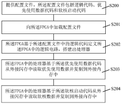
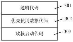
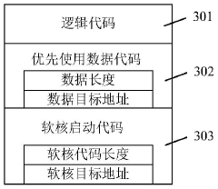
Initialization method of external memory based on FPGA
PatentActiveCN114327660B
Innovation
- Provides an FPGA-based external memory initialization method. By loading the configuration file, including logic code, priority data code and soft core startup code, the priority data code is loaded into the external memory before the soft core data, ensuring that the application External devices can use priority data before the program is started, thereby improving the human-computer interaction experience and system operating efficiency.
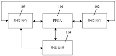
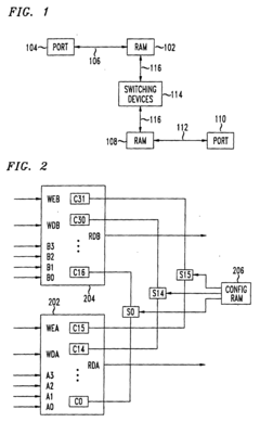
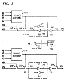
Field programmable gate array with multi-port RAM
PatentInactiveEP0756383B1
Innovation
- An FPGA design utilizing programmable switching devices to couple and decouple RAM cells, allowing them to function as single-port RAMs individually or collectively as dual-port RAMs, enabling simultaneous read and write operations at both ports.
Power Efficiency Considerations in DDR5-FPGA Systems
Power consumption has emerged as a critical factor in DDR5-FPGA system design, with significant implications for overall system performance and operational costs. DDR5 memory introduces advanced power management features that, when properly integrated with FPGA designs, can yield substantial efficiency improvements over previous memory generations. The voltage reduction from DDR4's 1.2V to DDR5's 1.1V represents a fundamental shift that delivers approximately 17% power savings in baseline operations.
FPGA designers must consider the new power architecture of DDR5, which separates the voltage rails for memory array (VDD) and input/output interfaces (VDDQ). This separation enables more granular power management and creates opportunities for dynamic voltage scaling based on workload demands. The implementation of voltage regulators on the memory module itself—rather than on the motherboard as in previous generations—allows for more precise power delivery and reduced power loss during transmission.
The power management state machine in DDR5 offers multiple low-power states that can be strategically utilized in FPGA designs. These include self-refresh, power-down, and multiple partial array self-refresh modes. FPGA controllers can be programmed to intelligently transition between these states based on memory access patterns, significantly reducing idle power consumption without compromising data availability when needed.
Thermal considerations have gained prominence in DDR5-FPGA systems due to increased operating frequencies and data rates. The integration of Temperature Event (TXR) signaling in DDR5 allows FPGAs to receive real-time temperature data from memory modules and adjust refresh rates or throttle operations accordingly. This capability prevents thermal-related failures while optimizing power consumption under varying environmental conditions.
Advanced FPGA power optimization techniques for DDR5 integration include clock gating for unused memory channels, intelligent refresh management, and workload-aware memory access scheduling. These techniques can be implemented through custom logic in the FPGA fabric or through vendor-provided IP cores that are specifically optimized for DDR5 interfaces.
The power efficiency gains from proper DDR5-FPGA integration translate directly to operational benefits in data centers and high-performance computing environments. Analysis of current implementations shows that optimized DDR5-FPGA systems can achieve 20-30% better performance-per-watt metrics compared to equivalent DDR4 systems. This efficiency improvement becomes particularly significant in large-scale deployments where power consumption directly impacts cooling requirements and operational expenditure.
Signal Integrity and Timing Closure Techniques
Signal integrity and timing closure represent critical challenges in DDR5 integration with FPGA designs. As DDR5 memory operates at significantly higher frequencies (up to 6400 MT/s) compared to previous generations, maintaining signal integrity becomes exponentially more complex. The reduced voltage swing of DDR5 (1.1V compared to DDR4's 1.2V) creates a smaller noise margin, making designs more susceptible to signal degradation.
Advanced PCB design techniques are essential for DDR5-FPGA integration. Controlled impedance routing with precise length matching becomes paramount, with tolerances typically under ±2 mils for critical DDR5 signals. Designers must implement proper termination schemes, including on-die termination (ODT) and series termination resistors, to minimize reflections that can cause signal integrity issues.
Timing closure techniques for DDR5-FPGA designs require sophisticated approaches to manage the reduced timing margins. The implementation of delay-locked loops (DLLs) and phase-locked loops (PLLs) within modern FPGAs helps compensate for clock skew and jitter. Advanced FPGA tools now offer specific DDR5 IP cores with built-in calibration mechanisms that automatically adjust timing parameters during initialization and operation.
Eye diagram analysis has become indispensable for DDR5-FPGA integration. These visual representations help engineers identify potential signal integrity issues by displaying the overlaid waveforms at the receiver. A clean "eye" with sufficient height and width indicates robust signal integrity, while a closed or distorted eye suggests problems requiring remediation.
Pre-emphasis and equalization techniques are increasingly employed to combat signal degradation over PCB traces. Pre-emphasis boosts the high-frequency components of signals at the transmitter, while equalization at the receiver compensates for channel losses. Modern FPGAs supporting DDR5 typically include programmable equalization circuits that can be fine-tuned for specific board layouts.
Power integrity considerations are tightly coupled with signal integrity in DDR5 designs. The increased switching speeds create significant power delivery network (PDN) challenges. Implementing adequate decoupling capacitors and power plane designs is critical to minimize power supply noise that can directly impact signal integrity and timing margins.
Simulation-based verification using tools like IBIS-AMI models has become standard practice for DDR5-FPGA designs. These simulations allow engineers to predict signal integrity issues before physical implementation, reducing design iterations and accelerating time-to-market. Advanced tools now support end-to-end channel simulation, accounting for package effects, PCB traces, and connector models.
Unlock deeper insights with PatSnap Eureka Quick Research — get a full tech report to explore trends and direct your research. Try now!
Generate Your Research Report Instantly with AI Agent
Supercharge your innovation with PatSnap Eureka AI Agent Platform!