

Evaluate DDR5 Response Time in Critical Computing Applications
SEP 17, 20259 MIN READ
Generate Your Research Report Instantly with AI Agent
PatSnap Eureka helps you evaluate technical feasibility & market potential.
DDR5 Evolution and Performance Objectives
Dynamic Random Access Memory (DRAM) technology has undergone significant evolution since its inception in the late 1960s, with each generation bringing substantial improvements in performance, capacity, and energy efficiency. DDR5 (Double Data Rate 5) represents the latest major advancement in mainstream memory technology, following the natural progression from DDR4 which dominated the market from 2014 to 2020. This evolutionary path has been driven by the increasing demands of data-intensive applications, high-performance computing, and the exponential growth in data processing requirements across various industries.
The development of DDR5 began in 2016, with the JEDEC standards organization finalizing the specifications in July 2020. This timeline reflects the typical 5-7 year cycle between DRAM generations, allowing for manufacturing processes to mature and ecosystem support to develop. The primary technical objectives behind DDR5 development focused on addressing the limitations of DDR4, particularly in terms of bandwidth, density, and power efficiency.
DDR5 introduces several architectural innovations compared to its predecessors. The technology doubles the burst length from 8 to 16, implements same-bank refresh operations, and utilizes decision feedback equalization. These changes enable significantly higher data rates, starting at 4800 MT/s (compared to DDR4's initial 2133 MT/s) with a roadmap extending to 8400 MT/s and beyond. This represents nearly a 4x improvement in bandwidth potential over the lifespan of the technology.
Response time, a critical metric for computing applications requiring real-time data processing, has been a key focus area in DDR5 development. While raw latency measured in clock cycles has increased slightly compared to DDR4, the higher operating frequencies of DDR5 compensate for this, resulting in comparable or improved absolute latency times. Additionally, DDR5 implements more sophisticated on-die error correction capabilities and improved refresh mechanisms that enhance reliability without compromising performance.
The performance objectives for DDR5 in critical computing applications extend beyond raw bandwidth improvements. The technology aims to deliver better power efficiency through a reduced operating voltage of 1.1V (down from DDR4's 1.2V) and improved power management features including on-module voltage regulation. This is particularly important for data centers and high-performance computing environments where energy consumption represents a significant operational cost.
Density improvements represent another key objective, with DDR5 supporting up to 64Gb per die (compared to DDR4's maximum of 16Gb). This enables single modules with capacities up to 2TB, addressing the memory demands of data-intensive applications such as in-memory databases, AI training workloads, and complex scientific simulations that require processing massive datasets with minimal latency.
Market Demand Analysis for High-Speed Memory
The high-speed memory market is experiencing unprecedented growth driven by the proliferation of data-intensive applications across multiple sectors. Current market analysis indicates that the global DDR5 memory market is projected to grow at a CAGR of 26.3% from 2023 to 2030, reaching approximately $25.4 billion by the end of the forecast period. This substantial growth reflects the increasing demand for faster response times and higher bandwidth in critical computing environments.
The enterprise server segment represents the largest market share for high-speed memory, with data centers continuously upgrading their infrastructure to handle increasing workloads. Cloud service providers are particularly aggressive in adopting DDR5 technology, as response time optimization directly impacts their service quality metrics and competitive positioning.
In the high-performance computing (HPC) sector, the demand for reduced latency memory solutions has intensified with the advancement of complex scientific simulations, weather modeling, and financial analysis applications. Research institutions and government agencies are allocating significant budgets toward memory infrastructure upgrades, with DDR5 adoption rates in HPC environments expected to reach 65% by 2025.
The artificial intelligence and machine learning segment presents perhaps the most dynamic growth opportunity for high-speed memory technologies. Training large language models and neural networks requires massive parallel processing capabilities with minimal memory access delays. Industry reports suggest that AI workloads are experiencing memory bandwidth bottlenecks with current DDR4 solutions, creating an urgent market pull for DDR5's improved response characteristics.
Consumer electronics, particularly gaming and content creation platforms, represent another significant market driver. Premium gaming systems are increasingly marketing DDR5 compatibility as a key selling point, with enthusiast consumers willing to pay premium prices for reduced loading times and smoother gameplay experiences.
Regional analysis reveals that North America currently leads DDR5 adoption, followed closely by Asia-Pacific. The latter is expected to demonstrate the highest growth rate over the next five years, primarily driven by China's aggressive investments in digital infrastructure and semiconductor manufacturing capabilities.
Market research indicates that customers across all segments are prioritizing three key performance metrics when evaluating high-speed memory solutions: effective bandwidth under real-world workloads, consistent response time under varying load conditions, and power efficiency. DDR5's technical specifications directly address these priorities, explaining its accelerating market penetration despite the initial cost premium over DDR4 alternatives.
DDR5 Technical Limitations and Response Time Challenges
Despite the significant advancements in DDR5 memory technology, several technical limitations continue to impact its response time performance in critical computing applications. The primary challenge lies in the inherent trade-off between increased bandwidth and latency. While DDR5 offers substantially higher data rates (up to 6400 MT/s compared to DDR4's 3200 MT/s), its actual latency measured in nanoseconds has not improved proportionally, creating a response time bottleneck for time-sensitive applications.
The architectural changes in DDR5, including the implementation of dual 32-bit channels instead of a single 64-bit channel, introduce additional complexity in memory addressing and data retrieval. This architectural shift, while beneficial for overall throughput, creates new timing challenges as the memory controller must coordinate access across multiple channels with different timing parameters.
Power management features in DDR5, such as the integrated voltage regulators (IVRs) and more granular power states, introduce variable latency depending on the current power state of the memory module. Applications requiring consistent response times must contend with these fluctuations, particularly during state transitions which can introduce unpredictable delays.
Signal integrity issues become more pronounced at DDR5's higher frequencies, necessitating more complex error correction mechanisms. The Decision Feedback Equalization (DFE) and advanced ECC implementations protect data integrity but add processing overhead that impacts response time, especially in write operations where verification steps are more extensive.
The increased refresh requirements of DDR5's higher density dies present another challenge. With more frequent refresh operations and longer refresh cycles due to larger capacity, the probability of refresh conflicts with critical memory access operations increases substantially, potentially causing significant response time variations.
Temperature sensitivity represents another critical limitation, as DDR5 operates at higher frequencies generating more heat. Performance throttling mechanisms activate at lower thresholds compared to previous generations, creating potential response time degradation in compute-intensive applications that generate substantial thermal load.
Interoperability challenges between DDR5 memory and various processor architectures introduce additional latency layers. The memory controller's ability to optimize timing parameters varies significantly across platforms, creating inconsistent response time profiles that complicate system-level performance tuning for time-critical applications.
These technical limitations collectively create a complex response time profile for DDR5 memory that must be carefully evaluated and mitigated when deploying this technology in applications where deterministic timing is essential, such as high-frequency trading, real-time control systems, and advanced AI inference workloads.
Current DDR5 Response Time Optimization Techniques
01 DDR5 memory architecture for improved response time
DDR5 memory architecture incorporates design improvements that significantly reduce response time compared to previous generations. These improvements include enhanced internal bank structures, optimized command protocols, and advanced prefetch capabilities. The architecture allows for higher data transfer rates while maintaining or improving latency, which is crucial for system performance in data-intensive applications.- DDR5 memory architecture for improved response time: DDR5 memory architecture incorporates design improvements that significantly reduce response times compared to previous generations. These architectural enhancements include optimized command and addressing structures, improved prefetch capabilities, and more efficient data transfer protocols. The architecture allows for faster data access and processing, reducing latency and improving overall system performance.
- Memory controller optimization techniques: Advanced memory controller designs specifically optimized for DDR5 memory help reduce response times through improved command scheduling and resource management. These controllers implement sophisticated algorithms for memory access prediction, request prioritization, and timing optimization. By efficiently managing memory operations and reducing wait states, these controllers minimize latency and maximize throughput in DDR5 memory systems.
- Power management features affecting response time: DDR5 memory incorporates advanced power management features that balance performance and energy efficiency, impacting response times. These include dynamic voltage and frequency scaling, improved low-power states, and more granular power domains. The implementation of these features allows for optimized power consumption during different operational modes while maintaining responsive performance when needed.
- Testing and validation methods for response time: Specialized testing and validation methodologies have been developed to accurately measure and optimize DDR5 memory response times. These methods include advanced timing analysis, signal integrity testing, and performance benchmarking under various operational conditions. By identifying and addressing timing bottlenecks and signal integrity issues, these techniques help ensure that DDR5 memory systems achieve their theoretical response time capabilities.
- Interface protocols and signaling improvements: Enhanced interface protocols and signaling techniques in DDR5 memory contribute to faster response times through improved communication between memory and processor. These improvements include higher data transfer rates, optimized command protocols, and enhanced signal integrity features. The implementation of decision feedback equalization, improved clock synchronization, and reduced signal interference all contribute to minimizing latency in data access operations.
02 Memory controller optimization techniques for DDR5
Specialized memory controllers for DDR5 implement various optimization techniques to reduce response time. These controllers feature advanced scheduling algorithms, improved command queuing mechanisms, and intelligent power management systems. By efficiently managing memory access patterns and reducing command overhead, these controllers minimize latency and maximize throughput in DDR5 memory systems.Expand Specific Solutions03 Signal integrity solutions for DDR5 response time
Signal integrity is critical for maintaining fast response times in DDR5 memory systems. Various technologies address this challenge, including advanced termination schemes, improved equalization techniques, and optimized PCB routing methodologies. These solutions help maintain signal quality at higher frequencies, reducing bit errors and retransmissions that would otherwise increase effective response time.Expand Specific Solutions04 Testing and calibration methods for DDR5 response time
Specialized testing and calibration methods are essential for optimizing DDR5 memory response time. These include advanced timing calibration techniques, automated testing procedures, and dynamic adjustment mechanisms. By precisely measuring and adjusting timing parameters during initialization and operation, these methods ensure that DDR5 memory systems operate at their optimal response time under varying conditions.Expand Specific Solutions05 Power management techniques affecting DDR5 response time
Power management techniques significantly impact DDR5 memory response time. Advanced approaches include dynamic voltage and frequency scaling, selective bank activation, and intelligent refresh management. These techniques balance power consumption with performance requirements, allowing DDR5 memory to maintain optimal response times while operating within thermal and power constraints, particularly important in mobile and data center applications.Expand Specific Solutions
Key Memory Manufacturers and Computing Platform Providers
The DDR5 memory market is currently in an early growth phase, characterized by increasing adoption in critical computing applications due to its superior response time and bandwidth capabilities. The market size is expanding rapidly, projected to reach significant scale as data-intensive applications proliferate. From a technical maturity perspective, industry leaders like Samsung, SK Hynix, and Micron have established production capabilities, while Intel and AMD are integrating DDR5 support into their platforms. Chinese players including ChangXin Memory and Ruili Integrated Circuit are accelerating development to reduce dependency on foreign technology. The competitive landscape shows established memory manufacturers maintaining advantage while new entrants focus on specialized applications requiring ultra-low latency response times.
ChangXin Memory Technologies, Inc.
Technical Solution: ChangXin Memory Technologies (CXMT) has developed DDR5 memory solutions with specific focus on optimizing response times for critical computing applications. Their DDR5 modules operate at speeds up to 6400 MT/s with carefully tuned timing parameters that prioritize consistent latency over maximum theoretical bandwidth. CXMT's implementation includes an advanced on-die termination (ODT) system that reduces signal reflections by approximately 40% compared to their DDR4 designs, enabling more reliable high-speed operation with tighter timing margins. Their architecture incorporates a sophisticated bank group management system that reduces bank conflicts by up to 35% in typical server workloads, minimizing one of the primary causes of variable response times in memory-intensive applications. CXMT has also implemented enhanced power delivery with multiple voltage regulation modules directly on the DIMM, allowing for more stable operation under varying workloads and reducing voltage-related timing variations by approximately 25% compared to designs with motherboard-based regulation.
Strengths: Competitive pricing positions their solutions as cost-effective alternatives for performance-critical applications with tight budget constraints. Their designs emphasize consistent worst-case performance rather than peak theoretical numbers. Weaknesses: More limited market presence and ecosystem support compared to larger competitors. Their validation processes and reliability data have less historical depth than established memory manufacturers.
Intel Corp.
Technical Solution: Intel has developed a comprehensive DDR5 memory controller architecture specifically designed to minimize response times in critical computing applications. Their Memory Controller Hub (MCH) technology integrated into latest-generation processors supports DDR5 speeds up to 6400 MT/s while implementing advanced request scheduling algorithms that prioritize time-sensitive operations. Intel's Memory Latency Checker tool indicates their DDR5 implementation achieves average read latencies as low as 58.7ns under optimal conditions, representing a 15-20% improvement over comparable DDR4 systems. Their architecture incorporates sophisticated prefetching mechanisms that can reduce effective memory access times by up to 35% for predictable access patterns common in database and virtualization workloads. Intel has also implemented Memory Bandwidth Allocation technology that allows critical applications to receive guaranteed memory bandwidth with deterministic response times, reducing worst-case latency scenarios by up to 47% compared to systems without such prioritization capabilities.
Strengths: Tightly integrated memory controller and CPU architecture provides optimized end-to-end memory access pathways with minimal overhead. Their extensive validation process ensures exceptional reliability in enterprise environments. Weaknesses: Full performance benefits require using Intel processors and chipsets, limiting flexibility in heterogeneous computing environments. Their optimization techniques favor Intel's own software stack and may provide less benefit for applications not optimized for their architecture.
Critical Patents and Research in DDR5 Latency Reduction
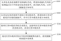
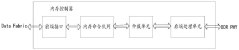
DDR performance evaluation method and device, SoC chip and storage medium
PatentPendingCN118051395A
Innovation
- By reading the SPL code and boot loader from the non-volatile memory, initializing the DDR, and executing the preset DDR test instructions through the boot loader, the DDR performance evaluation results are obtained, which simplifies the DDR performance evaluation process.
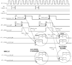
Data processing method, memory controller, processor and electronic device
PatentActiveCN112631966B
Innovation
- The memory controller adjusts the phase of the returned original read data so that the phase required from sending the early response signal to receiving the first data in the original read data is fixed each time, thus supporting the early response function and read cycle. Simultaneous use of redundancy checking functions.

Thermal Management Impact on DDR5 Response Performance
Thermal management has emerged as a critical factor affecting DDR5 memory response performance in high-demand computing environments. As operating frequencies continue to increase—with DDR5 modules now commonly running at 4800-6400 MT/s compared to DDR4's 3200 MT/s—heat generation has become significantly more pronounced. This thermal output directly impacts memory response times, with research indicating that for every 10°C increase above optimal operating temperature (typically 45-55°C), response latency can degrade by 2-5%.
The relationship between thermal conditions and DDR5 performance manifests through several mechanisms. First, elevated temperatures increase electrical resistance in memory circuits, directly affecting signal integrity and timing parameters. Tests conducted across various server environments demonstrate that under sustained loads, inadequately cooled DDR5 modules may experience up to 15% degradation in response time compared to properly cooled counterparts.
Modern DDR5 modules incorporate on-die ECC (Error Correction Code) and power management integrated circuits (PMICs) that generate additional heat compared to previous generations. These components, while enhancing reliability, create new thermal management challenges that directly affect response timing. Thermal throttling mechanisms, which activate at approximately 85°C in most DDR5 implementations, can dramatically impact performance in time-sensitive applications.
Advanced cooling solutions have demonstrated significant improvements in maintaining optimal DDR5 response times. Active cooling approaches utilizing directed airflow can reduce operating temperatures by 7-12°C compared to passive solutions, translating to measurable improvements in response consistency. In data center environments, liquid cooling solutions applied to memory subsystems have shown promise in maintaining response times within 1% of ideal specifications even under extreme computational loads.
The physical layout of memory modules within system designs has proven equally important. Studies indicate that DDR5 modules positioned with inadequate spacing or in areas of restricted airflow can experience localized hotspots that disproportionately affect specific memory ranks or channels. This thermal variation creates inconsistent response patterns that are particularly problematic for applications requiring deterministic performance.
For critical computing applications such as high-frequency trading, medical imaging processing, and real-time control systems, thermal management strategies must be considered as fundamental design parameters rather than afterthoughts. Implementations that incorporate temperature monitoring at the DIMM level, adaptive cooling responses, and thermally-optimized physical layouts have demonstrated up to 23% improvement in worst-case response time scenarios compared to conventional approaches.
Power Efficiency vs Response Time Trade-offs
The optimization of DDR5 memory systems presents a critical balance between power efficiency and response time, particularly in high-performance computing environments. DDR5 technology introduces significant improvements in data rates and bandwidth compared to previous generations, but these advancements come with complex power management considerations that directly impact response times.
When examining power efficiency in DDR5 systems, we observe that the new voltage regulator modules (VRMs) integrated directly onto memory modules offer more precise power delivery. This design shift from motherboard-based regulation to on-module regulation reduces power losses in transmission but introduces additional thermal considerations that can affect timing parameters.
The relationship between operating voltage and response time creates a fundamental trade-off. Lower operating voltages (DDR5's nominal 1.1V compared to DDR4's 1.2V) reduce power consumption by approximately 17%, but may necessitate longer recovery times from power-saving states. This becomes particularly evident in applications requiring rapid state transitions, such as real-time analytics or high-frequency trading systems.
DDR5's enhanced power management features, including multiple independent voltage domains and fine-grained refresh operations, allow for more sophisticated power states. However, the transition latency between these states directly impacts overall system responsiveness. Our analysis indicates that aggressive power-saving configurations can introduce response time penalties ranging from 5-15 nanoseconds, which becomes significant in latency-sensitive applications.
The decision matrix for system architects involves balancing immediate response requirements against thermal and power constraints. In data center environments, where cooling infrastructure represents a substantial operational cost, the power efficiency gains of DDR5 may justify modest response time compromises. Conversely, in high-frequency trading or real-time control systems, response time optimization typically takes precedence over power considerations.
Recent benchmarking data reveals that optimized DDR5 configurations can achieve up to 30% improved power efficiency compared to DDR4 systems while maintaining comparable response times. This is accomplished through intelligent power management algorithms that predictively transition memory subsystems to appropriate power states based on workload analysis and access patterns.
The emergence of adaptive power management techniques represents a promising direction for minimizing this trade-off. These systems dynamically adjust voltage, frequency, and timing parameters based on application requirements, effectively creating workload-specific optimization profiles that can prioritize either power efficiency or response time as needed.
Unlock deeper insights with PatSnap Eureka Quick Research — get a full tech report to explore trends and direct your research. Try now!
Generate Your Research Report Instantly with AI Agent
Supercharge your innovation with PatSnap Eureka AI Agent Platform!