

Electrochemical And Mechanical Compatibility With PCB Materials
AUG 22, 20259 MIN READ
Generate Your Research Report Instantly with AI Agent
PatSnap Eureka helps you evaluate technical feasibility & market potential.
PCB Material Compatibility Background and Objectives
The evolution of printed circuit boards (PCBs) has been a cornerstone of electronic device miniaturization and functionality enhancement since their inception in the early 20th century. From single-sided boards to today's complex multilayer designs, PCB technology has continuously adapted to meet increasing demands for higher performance, reliability, and durability across diverse operating environments. The compatibility between PCB materials and their electrochemical and mechanical properties has become increasingly critical as electronic devices face more challenging conditions including extreme temperatures, humidity, vibration, and chemical exposure.
The historical progression of PCB materials reflects this adaptation, moving from early phenolic resin boards to modern high-performance substrates like polyimide and ceramic composites. This evolution has been driven by the need to support higher component densities, faster signal speeds, and greater thermal management capabilities while maintaining structural integrity and electrical performance over extended product lifecycles.
Current industry trends indicate a growing emphasis on environmentally sustainable materials that comply with regulations such as RoHS and REACH, while simultaneously meeting heightened performance requirements. The convergence of these factors has created a complex landscape where material selection must balance technical performance, regulatory compliance, cost considerations, and environmental impact.
The primary objective of this technical research is to comprehensively evaluate the electrochemical and mechanical compatibility issues between various PCB materials and their operating environments. This includes analyzing how different substrate materials, solder masks, surface finishes, and conductive elements interact under various conditions, and how these interactions affect long-term reliability and performance.
Specifically, this research aims to identify optimal material combinations that minimize electrochemical degradation mechanisms such as galvanic corrosion, conductive anodic filament (CAF) formation, and electrochemical migration while maintaining mechanical stability against thermal cycling, vibration, and physical stress. The investigation will encompass both established materials and emerging alternatives, with particular attention to their behavior in harsh environments and high-reliability applications.
By establishing a clear understanding of these compatibility factors, this research seeks to develop predictive models and design guidelines that can inform material selection decisions, manufacturing processes, and quality control measures. The ultimate goal is to enable the development of more resilient, longer-lasting electronic systems while reducing field failures and warranty claims related to material compatibility issues.
Market Analysis of Electrochemical Compatible PCB Materials
The global market for electrochemical and mechanically compatible PCB materials is experiencing robust growth, driven primarily by the expanding electronics industry and increasing demand for reliable, high-performance circuit boards across multiple sectors. Current market valuations place this segment at approximately 9.7 billion USD in 2023, with projections indicating a compound annual growth rate of 4.8% through 2028.
The automotive sector represents one of the fastest-growing application areas, particularly with the rapid expansion of electric vehicles requiring PCB materials that can withstand harsh operating environments while maintaining electrochemical stability. This segment alone accounts for nearly 22% of the total market share and is expected to grow significantly as automotive electrification accelerates globally.
Consumer electronics continues to be the largest application segment, comprising roughly 35% of the market. The miniaturization trend in smartphones, wearables, and portable devices has intensified the need for PCB materials that offer superior electrochemical compatibility while maintaining mechanical integrity under increasingly compact designs.
Regional analysis reveals Asia-Pacific as the dominant market, controlling approximately 58% of global production and consumption. China, Taiwan, and South Korea lead manufacturing capacity, though recent supply chain diversification efforts have boosted production capabilities in Vietnam, Malaysia, and India. North America and Europe together account for roughly 32% of the market, with particular strength in high-reliability applications for aerospace, defense, and medical devices.
The market structure shows moderate concentration, with the top five suppliers controlling approximately 47% of global capacity. These major players have established significant barriers to entry through proprietary material formulations and process technologies that enhance electrochemical compatibility while maintaining mechanical performance.
Pricing trends indicate moderate volatility, influenced by fluctuations in raw material costs, particularly copper, epoxy resins, and specialty chemicals. The average selling price for high-performance electrochemically compatible PCB materials has seen a 3.2% annual increase over the past three years, reflecting both rising input costs and growing demand for premium solutions.
Customer demand patterns show increasing preference for materials offering extended operational lifespans, reduced electrochemical migration potential, and enhanced thermal cycling resistance. This shift has created premium market segments where manufacturers can command price premiums of 15-30% for materials with superior electrochemical and mechanical compatibility profiles.
Current Challenges in PCB Electrochemical and Mechanical Compatibility
The PCB industry currently faces significant electrochemical and mechanical compatibility challenges that impede advancement in high-performance electronic systems. Electrochemical compatibility issues primarily manifest as corrosion, metal migration, and conductive anodic filament (CAF) formation. These phenomena accelerate in high-humidity environments and under bias voltage conditions, causing intermittent failures that are difficult to diagnose and potentially catastrophic to system reliability.
Material degradation represents another critical challenge, with PCB substrates experiencing decomposition when exposed to processing chemicals during manufacturing. This degradation compromises structural integrity and electrical performance, particularly in high-frequency applications where signal integrity depends heavily on material stability. The industry struggles to develop materials that maintain consistent dielectric properties across varying environmental conditions.
Thermal management presents a multifaceted challenge as modern electronic components generate significant heat during operation. Coefficient of thermal expansion (CTE) mismatches between PCB materials and mounted components lead to mechanical stress during thermal cycling, resulting in solder joint fatigue and eventual failure. This issue becomes particularly pronounced in applications requiring wide temperature operating ranges or frequent power cycling.
Miniaturization trends exacerbate these challenges by reducing feature sizes and increasing component density. As trace widths and spacing decrease, electrochemical migration risks increase exponentially. The industry faces significant difficulties in maintaining mechanical stability in thinner substrates while simultaneously improving thermal dissipation capabilities.
Environmental compliance adds another layer of complexity as regulations increasingly restrict hazardous substances in electronic products. The transition from traditional lead-based solders to lead-free alternatives has introduced new compatibility challenges, including higher processing temperatures that stress PCB materials and altered surface finishes that may exhibit different electrochemical behaviors.
Manufacturing process compatibility represents a persistent challenge as new materials must integrate with established production methods. Novel substrate materials offering improved electrical or thermal properties often require specialized handling or processing techniques that disrupt existing manufacturing workflows, creating barriers to adoption despite their technical advantages.
The increasing adoption of flexible and rigid-flex PCBs introduces unique compatibility challenges related to mechanical stress during bending and folding operations. These designs must maintain electrical integrity through repeated mechanical deformation while resisting delamination and conductor cracking, requiring specialized material formulations and manufacturing techniques.
Existing PCB Material Compatibility Solutions and Approaches
01 Electrochemical compatibility of PCB materials
Electrochemical compatibility is crucial for PCB materials to prevent corrosion and ensure long-term reliability. This involves selecting materials that minimize galvanic reactions when different metals come into contact in the presence of an electrolyte. Proper material selection and surface treatments can significantly reduce electrochemical degradation, extending the lifespan of electronic components. Specialized coatings and plating techniques are employed to create barriers against environmental factors that could trigger electrochemical reactions.- Electrochemical compatibility of PCB materials: Electrochemical compatibility is crucial for PCB materials to prevent corrosion and ensure long-term reliability. This involves selecting materials that minimize galvanic reactions when different metals come into contact in the presence of an electrolyte. Proper material selection and surface treatments can significantly reduce electrochemical degradation, extending the lifespan of electronic components. Techniques such as electroplating and surface passivation are employed to enhance the electrochemical compatibility of PCB materials.
- Mechanical durability and stress resistance of PCB materials: PCB materials must exhibit sufficient mechanical durability to withstand various stresses during manufacturing, assembly, and operation. This includes resistance to bending, vibration, thermal cycling, and impact forces. Materials with appropriate flexibility, tensile strength, and adhesion properties are selected to ensure mechanical compatibility with other components. Reinforced substrates and specialized laminates are used to enhance the mechanical properties of PCBs, preventing delamination and fracture under stress conditions.
- Thermal management and material compatibility: Thermal compatibility is essential for PCB materials to maintain structural integrity and electrical performance across operating temperature ranges. Materials with matched coefficients of thermal expansion help prevent warping, cracking, and connection failures during thermal cycling. Advanced thermal management solutions incorporate heat-dissipating materials and structures to maintain optimal operating temperatures. Proper material selection ensures that components can withstand thermal stresses without compromising electrochemical or mechanical properties.
- Polymer and composite materials for enhanced compatibility: Specialized polymers and composite materials are developed to provide superior electrochemical and mechanical compatibility in PCB applications. These materials offer improved chemical resistance, reduced moisture absorption, and enhanced dimensional stability. Polymer composites can be engineered with specific properties to meet the demands of high-performance electronic applications. The incorporation of fillers and reinforcements in these materials can significantly improve their thermal, mechanical, and electrical characteristics while maintaining compatibility with other PCB components.
- Testing and evaluation methods for material compatibility: Various testing and evaluation methods are employed to assess the electrochemical and mechanical compatibility of PCB materials. These include accelerated aging tests, environmental stress testing, thermal cycling, and mechanical stress analysis. Advanced analytical techniques such as impedance spectroscopy and surface analysis help identify potential compatibility issues before they cause failures. Standardized testing protocols ensure that materials meet industry requirements for reliability and performance under various operating conditions.
02 Mechanical durability and stress resistance in PCB materials
PCB materials must withstand various mechanical stresses during manufacturing, assembly, and operation. This includes resistance to bending, vibration, thermal expansion, and physical impact. Advanced composite materials are developed to enhance mechanical properties while maintaining electrical performance. Reinforcement techniques such as glass fiber integration and specialized lamination processes improve the structural integrity of PCBs. These materials are designed to maintain dimensional stability under varying environmental conditions and mechanical loads.Expand Specific Solutions03 Thermal management and material compatibility
Thermal compatibility between different PCB materials is essential for preventing delamination, warping, and other failures caused by thermal stress. Materials with matched coefficients of thermal expansion help maintain structural integrity during temperature fluctuations. Advanced thermal management solutions incorporate heat-dissipating materials and structures to efficiently transfer heat away from sensitive components. These materials must maintain their mechanical and electrical properties across the operational temperature range while providing adequate thermal conductivity.Expand Specific Solutions04 Chemical resistance and environmental stability
PCB materials must resist degradation from exposure to chemicals during manufacturing processes and in operational environments. This includes resistance to cleaning solvents, flux residues, atmospheric pollutants, and moisture. Specialized polymers and protective coatings are developed to enhance chemical resistance while maintaining electrical performance. Environmental stability ensures that PCB materials maintain their properties under varying humidity, temperature, and atmospheric conditions, preventing premature failure due to material degradation.Expand Specific Solutions05 Advanced composite materials for enhanced compatibility
Novel composite materials are being developed to simultaneously address electrochemical and mechanical compatibility challenges in PCBs. These materials combine organic and inorganic components to achieve optimal electrical, thermal, and mechanical properties. Nano-enhanced composites incorporate particles that improve specific performance aspects while maintaining overall compatibility. These advanced materials often feature self-healing properties or adaptive characteristics that respond to environmental changes, extending PCB lifespan and reliability in demanding applications.Expand Specific Solutions
Leading Manufacturers and Suppliers in PCB Material Industry
The electrochemical and mechanical compatibility with PCB materials market is currently in a growth phase, with increasing demand driven by miniaturization trends in electronics. The global market is estimated at $5-7 billion annually, expanding at approximately 6-8% CAGR. Technologically, the field shows moderate maturity with ongoing innovation. Leading players include Samsung Electro-Mechanics and Hon Hai Precision, who focus on high-performance PCB materials, while Huawei and Bosch are advancing integration technologies. Research institutions like Beihang University and University of Minho contribute fundamental research. Specialized companies such as Liquid Wire and Shenzhen Suntak are developing novel solutions for flexible electronics applications, while TopFlex and Ciena are optimizing materials for telecommunications infrastructure, collectively driving improvements in reliability and performance.
Samsung Electro-Mechanics Co., Ltd.
Technical Solution: Samsung Electro-Mechanics has developed advanced High-Density Interconnect (HDI) PCB technology with optimized electrochemical compatibility through their proprietary Surface Treatment Technology (STT). This process involves precise control of copper surface roughness at the nano-scale level to enhance adhesion between copper traces and dielectric materials while minimizing electrochemical migration risks. Their multi-layer ceramic capacitor (MLCC) integration approach uses specialized conductive pastes with matched thermal expansion coefficients to prevent delamination during thermal cycling. Samsung's material selection protocol incorporates halogen-free substrates with enhanced thermal stability up to 180°C, significantly reducing the risk of conductive anodic filament (CAF) formation. Their PCBs feature controlled impedance designs with ±7% tolerance, achieved through advanced electroplating techniques that maintain uniform copper distribution even in high-aspect-ratio microvias.
Strengths: Superior electrochemical migration resistance through proprietary surface treatments; excellent thermal cycling reliability (up to 1000 cycles); and industry-leading miniaturization capabilities with 30μm line/space technology. Weaknesses: Higher manufacturing costs compared to standard PCB technologies; limited compatibility with some legacy components; requires specialized manufacturing equipment not widely available in the industry.
Huawei Technologies Co., Ltd.
Technical Solution: Huawei has pioneered a comprehensive PCB material compatibility system called "Electrochemical Reliability Enhancement Framework" (EREF) specifically designed for high-density, high-frequency applications in telecommunications equipment. Their approach integrates material science and manufacturing process optimization to address electrochemical and mechanical challenges. The EREF system employs a three-layer protection strategy: first, utilizing modified epoxy resin systems with nano-silica reinforcement (0.5-1.0% by weight) to enhance mechanical strength; second, implementing ion-trapping additives that chemically bind with metallic ions to prevent migration; and third, applying hydrophobic surface treatments that maintain a contact angle >110° even after multiple reflow cycles. Huawei's PCB designs incorporate specialized via structures with stress-relief features that accommodate CTE mismatches between components and substrates. Their manufacturing process includes precise control of electroplating parameters, maintaining current density variations below 10% across the board surface to ensure uniform metal deposition and prevent stress concentration points.
Strengths: Exceptional resistance to harsh environmental conditions (95% humidity at 65°C for 1000 hours without significant degradation); superior signal integrity in high-frequency applications up to 40GHz; and excellent thermal management capabilities. Weaknesses: Proprietary materials require specialized handling procedures; higher initial production costs; limited third-party manufacturing support for their most advanced designs.
Key Innovations in Electrochemical Resistant PCB Materials
Resin composition, circuit material containing same and printed circuit board
PatentPendingCN117777567A
Innovation
- Using low molecular weight and medium molecular weight thermosetting resin compositions with unsaturated double bonds, combined with spherical silica fillers and specific initiators, and controlling the proportion of resin and fillers, a product with stable dielectric constant, low dielectric loss and high peeling is prepared Strong circuit material.
Resin composition, preg, circuit board and printed circuit board
PatentActiveCN111440364A
Innovation
- A resin composition is used, including vinyl thermosetting resin, modified filler and curing agent. The surface of the filler is modified by a third resin to improve the compatibility and cross-linking density of the resin composition, form chemical bonds, and enhance dielectric properties. and mechanical strength, and can release stress during processing, bear force evenly, and optimize hole wall roughness.
Environmental Impact of PCB Material Selection
The selection of PCB materials has significant environmental implications throughout the entire lifecycle of electronic products. Traditional PCB manufacturing processes involve numerous hazardous chemicals and materials that pose substantial environmental risks. FR-4, the most commonly used PCB substrate, contains brominated flame retardants that can release toxic compounds when improperly disposed of or incinerated. These compounds may persist in the environment and bioaccumulate in living organisms, causing long-term ecological damage.
Water pollution represents another critical environmental concern in PCB production. The electroplating processes used to create conductive pathways generate heavy metal waste, including copper, nickel, and lead. Without proper treatment systems, these contaminants can leach into groundwater and surface water, disrupting aquatic ecosystems and potentially entering the human food chain.
Energy consumption during PCB manufacturing contributes significantly to the carbon footprint of electronic devices. The high-temperature processes required for lamination and curing consume substantial amounts of electricity, often derived from fossil fuel sources. This energy intensity translates directly into greenhouse gas emissions that accelerate climate change.
Recent regulatory frameworks, such as the European Union's Restriction of Hazardous Substances (RoHS) and Registration, Evaluation, Authorization and Restriction of Chemicals (REACH), have driven innovation toward more environmentally compatible PCB materials. Lead-free solders, halogen-free laminates, and water-soluble fluxes represent important advances in reducing the environmental impact of PCB production.
Emerging bio-based and biodegradable PCB materials offer promising alternatives to conventional petroleum-derived substrates. Materials derived from renewable resources such as cellulose, lignin, and plant-based epoxies can significantly reduce the carbon footprint of PCB manufacturing while maintaining necessary electrochemical and mechanical properties. These materials also present improved end-of-life scenarios, with greater potential for biodegradation or recycling.
The recyclability of PCB materials remains a significant challenge due to the heterogeneous nature of circuit boards. Improving design for disassembly and implementing modular approaches can enhance material recovery rates. Advanced recycling technologies, including pyrolysis and hydrometallurgical processes, are being developed to more effectively separate and recover valuable materials from PCB waste, reducing the environmental burden of electronic waste disposal.
Reliability Testing Standards for PCB Material Compatibility
Reliability testing standards for PCB material compatibility have evolved significantly over the past decades to address the increasing complexity of electronic systems and their operating environments. These standards provide systematic methodologies to evaluate how printed circuit board materials interact with various components under different conditions, ensuring long-term reliability and performance.
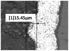
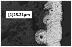
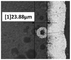
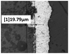
The IPC (Association Connecting Electronics Industries) has established several key standards that form the backbone of PCB material compatibility testing. IPC-TM-650 provides test methods for evaluating electrochemical migration resistance, which is critical for preventing conductive filament formation between traces. This standard includes specific protocols for temperature-humidity-bias (THB) testing, which accelerates potential electrochemical reactions between PCB materials and components.
ASTM D3359 and IPC-SM-840 standards address adhesion testing between PCB substrates and coatings, ensuring mechanical compatibility under thermal stress and physical manipulation. These tests typically involve cross-hatch cutting followed by tape testing to evaluate coating adhesion strength to the substrate material.
For environmental reliability, IPC-9701 provides guidelines for temperature cycling tests that evaluate the compatibility of PCB materials with soldered components during thermal expansion and contraction cycles. This is complemented by IPC-9704, which focuses on the mechanical shock and vibration resistance of assembled PCBs.
The automotive industry has developed more stringent standards through AEC-Q200, which includes specific requirements for PCB material compatibility testing under extreme temperature ranges (-40°C to +125°C) and high humidity conditions. These tests are particularly relevant for evaluating electrochemical stability in harsh environments.
Salt spray testing according to ASTM B117 evaluates corrosion resistance of PCB materials and their compatibility with protective coatings. This test is especially important for applications in marine or industrial environments where salt and other corrosive elements are present.
More recently, standards have evolved to address lead-free soldering compatibility issues. J-STD-020 provides guidelines for moisture sensitivity classification and reflow profiles that ensure PCB materials can withstand the higher temperatures required for lead-free assembly without delamination or other failures.
Insulation resistance testing per IPC-TM-650 method 2.6.3 evaluates how PCB materials maintain their electrical isolation properties when exposed to moisture and bias voltage, directly addressing electrochemical compatibility concerns in high-reliability applications.
Unlock deeper insights with PatSnap Eureka Quick Research — get a full tech report to explore trends and direct your research. Try now!
Generate Your Research Report Instantly with AI Agent
Supercharge your innovation with PatSnap Eureka AI Agent Platform!