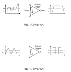
How to Achieve Ideal Schmitt Trigger Waveform Characteristics
SEP 23, 20259 MIN READ
Generate Your Research Report Instantly with AI Agent
Patsnap Eureka helps you evaluate technical feasibility & market potential.
Schmitt Trigger Evolution and Design Objectives
The Schmitt trigger, first introduced by Otto Schmitt in 1937, represents a significant milestone in electronic circuit design. Originally developed to mimic the neural impulse propagation in squid nerves, this hysteresis-based comparator has evolved into a fundamental building block in modern electronics. The evolution of Schmitt triggers has been marked by continuous refinements aimed at achieving more precise switching characteristics and greater noise immunity.
Early implementations relied on vacuum tubes, transitioning to discrete transistors in the 1950s and 1960s. The integration of Schmitt triggers into monolithic integrated circuits during the 1970s represented a pivotal advancement, enabling widespread adoption across diverse applications. Contemporary designs leverage advanced semiconductor technologies, including CMOS and BiCMOS processes, to achieve superior performance metrics while minimizing power consumption.
The primary technical objective in Schmitt trigger design centers on achieving ideal waveform characteristics. This encompasses several critical parameters: precise and consistent threshold voltages, minimal propagation delay, sharp transition edges, and excellent noise immunity. The hysteresis window—defined as the difference between upper and lower threshold voltages—must be optimally calibrated to prevent false triggering while maintaining responsiveness to legitimate signal transitions.
Temperature stability represents another crucial design objective, as threshold voltages in conventional implementations tend to drift with temperature variations. Modern applications demand Schmitt triggers that maintain consistent performance across industrial temperature ranges (-40°C to +85°C) or even extended ranges for automotive and military applications.
Power efficiency has emerged as an increasingly important consideration, particularly for battery-powered and energy-harvesting systems. Designers now target sub-microwatt operation while preserving switching performance, requiring innovative circuit topologies and careful transistor sizing.
The miniaturization trend in electronics has driven efforts to reduce the silicon footprint of Schmitt trigger implementations. This objective often conflicts with other performance goals, necessitating sophisticated design tradeoffs. Advanced process nodes enable more compact designs but introduce challenges related to process variations and reduced supply voltages.
Looking forward, emerging applications in ultra-low-power IoT devices, high-speed data conversion, and mixed-signal processing continue to push the boundaries of Schmitt trigger design. The technical evolution trajectory points toward programmable hysteresis, self-calibrating architectures, and integration with advanced digital processing for adaptive threshold adjustment based on environmental conditions and signal characteristics.
Market Applications and Industry Requirements
Schmitt trigger technology has established itself as a critical component across multiple industries due to its unique ability to provide clean signal transitions with built-in hysteresis. In the semiconductor market, the demand for Schmitt triggers with ideal waveform characteristics has grown significantly, particularly in sectors requiring precise signal conditioning and noise immunity. The automotive industry represents one of the largest application areas, with an estimated market value exceeding $3 billion for electronic components featuring Schmitt trigger functionality, as vehicles increasingly incorporate advanced driver assistance systems and electronic control units requiring reliable signal processing.
Consumer electronics manufacturers have similarly embraced Schmitt trigger technology, particularly in portable devices where power efficiency and signal integrity are paramount concerns. Market research indicates that devices with optimized Schmitt trigger characteristics can achieve up to 15% better power efficiency in certain applications, creating a significant competitive advantage in battery-powered products. This has driven demand for Schmitt triggers with precisely tailored hysteresis windows and switching thresholds.
Industrial automation represents another critical market segment, where Schmitt triggers are essential components in sensor interfaces, control systems, and safety equipment. The industrial IoT revolution has further accelerated demand for robust signal conditioning solutions that can operate reliably in electrically noisy environments. Industry specifications typically require Schmitt triggers with hysteresis ranges between 0.2V and 1.5V, depending on the specific application, with extremely fast transition times below 50ns.
Medical device manufacturers have established particularly stringent requirements for Schmitt trigger performance, especially in diagnostic and monitoring equipment where signal integrity directly impacts diagnostic accuracy. These applications demand Schmitt triggers with extremely low temperature drift characteristics and highly predictable threshold voltages across operating conditions.
The telecommunications sector has emerged as another significant consumer of high-performance Schmitt trigger technology, particularly in network infrastructure equipment where signal integrity across high-speed data paths is critical. Industry standards in this sector typically specify maximum allowable jitter figures that directly influence Schmitt trigger design parameters.
Aerospace and defense applications represent a smaller but premium market segment with the most demanding specifications for Schmitt trigger performance, including radiation hardening, extended temperature operation, and ultra-high reliability requirements. These applications often require custom-designed Schmitt trigger solutions with comprehensive documentation of performance characteristics across all operating conditions.
Technical Challenges in Schmitt Trigger Implementation
Despite significant advancements in Schmitt trigger design, several technical challenges persist in achieving ideal waveform characteristics. The primary challenge lies in maintaining consistent hysteresis width across varying operating conditions. Temperature fluctuations, supply voltage variations, and process variations in semiconductor manufacturing can all cause the hysteresis window to drift, resulting in unpredictable switching thresholds and compromised noise immunity.
Another significant challenge is the trade-off between switching speed and power consumption. Fast switching Schmitt triggers typically require higher current consumption, which becomes problematic in low-power applications such as IoT devices and battery-operated systems. Designers must carefully balance these competing requirements based on application-specific needs.
Noise susceptibility remains a persistent issue, particularly in industrial environments with high electromagnetic interference. While Schmitt triggers are inherently designed to reject noise, achieving optimal noise immunity without sacrificing other performance parameters requires sophisticated circuit techniques and layout considerations.
The asymmetry in rising and falling edge response times presents another design challenge. Ideally, a Schmitt trigger should exhibit symmetrical behavior for both transitions, but parasitic capacitances and inherent semiconductor characteristics often create disparities. This asymmetry can lead to duty cycle distortion in high-frequency applications and timing errors in precision measurement systems.
Input capacitance effects can significantly impact the waveform characteristics, especially at high frequencies. The input capacitance interacts with the source impedance to create an RC filter effect that can distort the input signal before it reaches the trigger threshold detection circuitry. Minimizing this effect requires careful input stage design and buffer implementation.
For integrated circuit implementations, process variations across different manufacturing batches can lead to inconsistent Schmitt trigger behavior. Designers must implement compensation techniques to ensure reliable operation across the entire range of process corners, which adds complexity to the design.
Power supply rejection ratio (PSRR) is another critical parameter that affects waveform quality. Poor PSRR allows power supply noise to couple into the trigger thresholds, causing jitter and false triggering. Implementing effective power supply filtering and reference voltage generation becomes essential but adds to design complexity.
Finally, achieving precise and programmable hysteresis levels presents significant challenges, especially when designing configurable Schmitt triggers for versatile applications. Implementing digitally controllable hysteresis requires additional circuitry that can introduce its own non-idealities and affect the overall performance of the trigger circuit.
Current Waveform Optimization Techniques
01 Hysteresis characteristics in Schmitt triggers
Schmitt triggers are characterized by hysteresis behavior, which provides different threshold voltages for rising and falling input signals. This hysteresis creates a noise margin that prevents unwanted oscillations when the input signal contains noise or has slow transition times. The difference between the upper and lower threshold voltages defines the hysteresis width, which can be adjusted through circuit design to meet specific application requirements.- Hysteresis characteristics in Schmitt triggers: Schmitt triggers are characterized by their hysteresis behavior, which provides different threshold voltages for rising and falling input signals. This hysteresis creates a noise margin that prevents unwanted oscillations when the input signal contains noise or slowly varying signals. The difference between the upper and lower threshold voltages defines the hysteresis width, which can be adjusted through circuit design to meet specific application requirements.
- Output waveform shaping and signal conditioning: Schmitt triggers excel at converting slowly changing input signals into sharp, well-defined digital output waveforms with fast transition times. This signal conditioning capability makes them ideal for cleaning up noisy signals and producing rectangular output waveforms with steep edges. The output characteristics can be tailored by adjusting circuit parameters to achieve desired rise/fall times and voltage levels, making them valuable in applications requiring clean digital signals from analog inputs.
- Frequency response and timing characteristics: The waveform characteristics of Schmitt triggers include specific timing behaviors such as propagation delay, rise/fall times, and frequency response limitations. These timing characteristics affect how the circuit responds to input signals of varying frequencies. Schmitt triggers can be designed with optimized frequency response for specific applications, with some implementations featuring enhanced high-frequency performance or controlled slew rates to manage electromagnetic interference.
- Temperature and voltage stability: Schmitt trigger waveform characteristics can be affected by temperature variations and supply voltage fluctuations. Advanced designs incorporate compensation techniques to maintain consistent threshold voltages and hysteresis windows across operating conditions. This stability ensures reliable switching behavior and consistent output waveforms even under varying environmental conditions, which is critical for applications in automotive, industrial, and outdoor environments.
- Implementation variations and their effect on waveforms: Different implementations of Schmitt triggers, such as CMOS, TTL, or discrete component designs, exhibit distinct waveform characteristics. These variations affect parameters like symmetry of hysteresis, power consumption, and noise immunity. Some implementations focus on low power consumption while others prioritize high-speed operation or rail-to-rail output swing. The choice of implementation technology significantly influences the resulting waveform characteristics and determines the circuit's suitability for specific applications.
02 Output waveform shaping and signal conditioning
Schmitt triggers are widely used for waveform shaping and signal conditioning, converting slowly changing input signals into clean square waves with sharp transitions. They effectively transform analog signals with gradual slopes into digital signals with well-defined logic levels. This characteristic makes them valuable in applications requiring clean digital signals from noisy or slowly varying inputs, improving signal integrity in digital systems.Expand Specific Solutions03 Threshold voltage control and adjustment
The threshold voltages of Schmitt triggers can be precisely controlled and adjusted through circuit design techniques. Various implementations allow for programmable or dynamically adjustable threshold levels to accommodate different input signal characteristics. Advanced designs incorporate temperature compensation and supply voltage independence to maintain consistent threshold levels across operating conditions, ensuring reliable triggering behavior in varying environments.Expand Specific Solutions04 Frequency response and timing characteristics
Schmitt triggers exhibit specific frequency response and timing characteristics that affect their performance in high-speed applications. The propagation delay between input and output transitions, rise and fall times of the output waveform, and maximum operating frequency are critical parameters. Enhanced designs focus on minimizing these delays while maintaining the noise immunity benefits, making them suitable for high-frequency applications where timing precision is essential.Expand Specific Solutions05 Implementation variations and circuit topologies
Various circuit topologies and implementation techniques exist for Schmitt triggers, each offering different waveform characteristics. These include CMOS, TTL, and BiCMOS implementations, as well as specialized designs for low-power applications. Different topologies provide trade-offs between power consumption, switching speed, noise immunity, and output drive capability. Advanced implementations incorporate features like rail-to-rail operation, reduced sensitivity to power supply variations, and optimized performance for specific application domains.Expand Specific Solutions
Leading Manufacturers and Research Institutions
The Schmitt trigger waveform technology market is currently in a growth phase, with increasing demand across various electronic applications requiring precise signal conditioning. The global market size for this technology is expanding steadily, driven by applications in industrial automation, consumer electronics, and telecommunications. From a technical maturity perspective, the field shows a blend of established principles and ongoing innovation. Leading academic institutions like University of Electronic Science & Technology of China and Shanghai Jiao Tong University are advancing fundamental research, while commercial players including QUALCOMM, Western Digital, and Samsung Electro-Mechanics are developing practical implementations with enhanced characteristics. Semiconductor Manufacturing International and Alphawave Semi are focusing on integration capabilities, while research organizations like Wisconsin Alumni Research Foundation are bridging theoretical advancements with commercial applications.
Semiconductor Manufacturing International (Shanghai) Corp.
Technical Solution: SMIC has developed cost-effective Schmitt trigger implementations optimized for their mainstream process nodes (28nm-180nm). Their approach focuses on balancing performance with manufacturing yield through careful design rule considerations. SMIC's standard cell libraries include multiple Schmitt trigger variants with different hysteresis specifications to address various application requirements. Their implementation utilizes traditional CMOS topologies with carefully optimized transistor sizing to achieve consistent hysteresis characteristics across process variations. For applications requiring tighter specifications, SMIC offers enhanced Schmitt trigger cells with trimming capabilities that can be adjusted during wafer testing. Recent developments include low-leakage variants specifically designed for IoT applications, incorporating power gating techniques and optimized threshold voltages to minimize standby current while maintaining noise immunity when active.
Strengths: Excellent cost-performance ratio suitable for high-volume applications; good manufacturing consistency across wafer lots; comprehensive characterization across operating conditions. Weaknesses: Performance specifications not as aggressive as leading-edge competitors; limited customization options compared to specialized providers; moderate temperature drift characteristics.
QUALCOMM, Inc.
Technical Solution: Qualcomm has developed advanced Schmitt trigger implementations for their mobile SoC designs, focusing on ultra-low power consumption while maintaining noise immunity. Their approach incorporates adaptive hysteresis control that dynamically adjusts threshold levels based on operating conditions. This technique utilizes specialized CMOS structures with optimized transistor sizing ratios to achieve precise switching characteristics. Qualcomm's designs typically employ differential input stages with carefully controlled feedback mechanisms to maintain consistent hysteresis windows across process variations and temperature fluctuations. Their latest implementations integrate programmable hysteresis settings that can be adjusted through digital control interfaces, allowing system-level optimization for different noise environments and power requirements.
Strengths: Superior noise immunity in mixed-signal environments; extremely low power consumption suitable for battery-powered devices; excellent process variation tolerance. Weaknesses: Proprietary designs limit broader industry adoption; implementation complexity increases silicon area requirements; may require calibration for optimal performance across temperature ranges.
Key Patents and Innovations in Hysteresis Control
Rapid transition schmitt trigger circuit
PatentActiveUS20150280694A1
Innovation
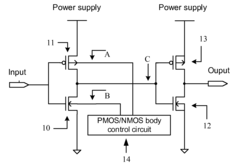
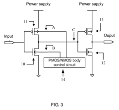
- A Schmitt trigger circuit with a PMOS/NMOS body control circuit, utilizing a first NMOS and PMOS transistor pair and a second NMOS and PMOS transistor pair, where the body region voltage of the transistors is controlled to change the flip-flop threshold voltage, reducing the number of transistors required for pull-up and pull-down operations and enhancing transition speed.
Schmitt Trigger Circuit With Hysteresis Determined By Modified Polysilicon Gate Dopants
PatentActiveUS20180097510A1
Innovation
- The implementation of Schmitt trigger circuits with two MOSFETs having identical source/drain/channel configurations but different polysilicon gate dopants, allowing for accurate and uniform hysteresis without the need for comparator or differential amplifier circuits and DC bias voltage, achieved by using standard and non-standard n-channel transistors with distinct threshold voltages.
Noise Immunity and Performance Metrics
Noise immunity represents a critical performance metric for Schmitt trigger circuits, directly influencing their reliability in real-world applications. The hysteresis characteristic of Schmitt triggers provides inherent noise rejection capabilities by requiring input signals to cross two distinct threshold voltages rather than a single threshold. This dual-threshold approach prevents output oscillations when the input signal contains noise components or experiences slow transition rates.
The noise margin of a Schmitt trigger is quantitatively defined by the hysteresis width—the voltage difference between the upper and lower threshold voltages (VTH and VTL). A wider hysteresis band improves noise immunity but may reduce sensitivity to legitimate signal transitions. Engineers must carefully balance this trade-off based on application requirements and expected noise environments.
Performance metrics for evaluating Schmitt trigger effectiveness include propagation delay, which measures the time between input threshold crossing and corresponding output response. This parameter becomes particularly important in high-speed applications where timing precision is critical. The slew rate, representing the maximum rate of change in the output voltage, constitutes another essential metric that affects the circuit's ability to produce clean transitions.
Power consumption represents a significant consideration, especially in battery-powered applications. Traditional CMOS Schmitt trigger implementations offer relatively low power consumption compared to bipolar alternatives, though specialized low-power designs may incorporate additional techniques such as dynamic threshold adjustment or power gating to further reduce energy requirements.
Temperature stability of threshold voltages directly impacts reliability across operating conditions. Well-designed Schmitt triggers maintain consistent hysteresis characteristics despite temperature variations, typically achieved through careful component selection and compensation techniques. Quantitative metrics like temperature coefficient of threshold voltages (measured in mV/°C) provide objective measures of this stability.
Frequency response characteristics determine the circuit's ability to process signals across different frequency bands. The bandwidth limitation of Schmitt triggers must be considered when implementing them in applications with high-frequency components. Advanced designs may incorporate frequency compensation techniques to extend usable bandwidth while maintaining noise immunity.
Measurement methodologies for these performance metrics typically involve specialized test setups that can precisely control input signal characteristics while monitoring output responses. Standard benchmarking procedures allow for objective comparison between different Schmitt trigger implementations, facilitating informed design decisions based on application-specific requirements.
Integration Challenges in Modern IC Design
The integration of Schmitt triggers into modern integrated circuit (IC) designs presents significant challenges that require careful consideration. As IC technologies continue to scale down to nanometer dimensions, the implementation of ideal Schmitt trigger characteristics becomes increasingly complex due to various physical constraints and design limitations.
Process variations in modern semiconductor manufacturing significantly impact the consistency of Schmitt trigger thresholds across chips. These variations can lead to unpredictable hysteresis windows, affecting the reliability of signal detection in noise-prone environments. Temperature sensitivity further complicates this issue, as the threshold voltages of Schmitt triggers can drift with changing operating temperatures, potentially compromising their noise immunity benefits.
Power consumption considerations have become paramount in contemporary IC design, particularly for mobile and IoT applications. Traditional Schmitt trigger circuits often consume more power than simple inverters due to their more complex structure and additional transistors. Designers must balance the need for robust noise immunity against stringent power budgets, often necessitating novel low-power Schmitt trigger architectures.
Area constraints represent another significant challenge, as the silicon real estate in modern ICs comes at a premium. Implementing full Schmitt trigger functionality in space-limited designs may require compromises in other circuit aspects or innovative layout techniques to maintain overall chip size targets while preserving critical noise immunity characteristics.
The increasing demand for higher operating frequencies in modern ICs also impacts Schmitt trigger performance. At high frequencies, parasitic capacitances and inductances can distort the ideal switching behavior, potentially reducing the effectiveness of the hysteresis window. Engineers must carefully model and simulate these high-frequency effects to ensure reliable operation across the intended frequency range.
Mixed-signal integration presents unique challenges when implementing Schmitt triggers at interfaces between analog and digital domains. Ensuring consistent trigger points while managing different voltage domains, ground noise, and substrate coupling requires sophisticated design approaches and often specialized layout techniques to maintain signal integrity across these boundaries.
As supply voltages continue to decrease in advanced process nodes, maintaining adequate noise margins becomes increasingly difficult. This trend directly impacts the design of Schmitt triggers, as the available voltage range for establishing meaningful hysteresis windows shrinks, potentially compromising their fundamental noise immunity advantage in ultra-low voltage applications.
Unlock deeper insights with Patsnap Eureka Quick Research — get a full tech report to explore trends and direct your research. Try now!
Generate Your Research Report Instantly with AI Agent
Supercharge your innovation with Patsnap Eureka AI Agent Platform!