

How to Improve WOLED Reliability Through Material Innovation
SEP 15, 20259 MIN READ
Generate Your Research Report Instantly with AI Agent
PatSnap Eureka helps you evaluate technical feasibility & market potential.
WOLED Reliability Evolution and Objectives
White Organic Light-Emitting Diodes (WOLEDs) have evolved significantly since their inception in the late 1990s. Initially, these devices suffered from severe reliability issues, with operational lifetimes measured in mere hundreds of hours. The primary degradation mechanisms included chemical decomposition of organic materials, interfacial instabilities, and electrode deterioration under electrical stress and environmental factors. Early WOLEDs exhibited rapid luminance decay, color shifts, and voltage drift that severely limited their commercial viability.
The evolution of WOLED reliability has been marked by several technological breakthroughs. The introduction of phosphorescent emitters in the early 2000s significantly improved quantum efficiency but presented new stability challenges. By the mid-2000s, the development of more stable host materials and improved device architectures led to substantial lifetime improvements, pushing operational stability to thousands of hours at display brightness levels.
Between 2010 and 2015, the industry witnessed the emergence of tandem structures and improved charge transport materials, which further enhanced device stability. The incorporation of electron and hole blocking layers optimized charge confinement and recombination efficiency, reducing operational stress on the emissive materials. These advancements collectively pushed WOLED lifetimes to tens of thousands of hours at standard brightness levels.
Recent years have seen the introduction of thermally activated delayed fluorescence (TADF) materials and hybrid emitter systems that combine the benefits of different emission mechanisms. These innovations have addressed specific degradation pathways while maintaining high efficiency. Additionally, improved encapsulation technologies have significantly reduced the impact of environmental factors such as moisture and oxygen on device degradation.
Despite these advancements, current WOLED technology still faces reliability challenges that limit broader adoption in certain applications. Blue emitters remain particularly problematic, with shorter lifetimes compared to their red and green counterparts. This color-dependent degradation leads to white point shifts over the operational lifetime of displays, affecting color accuracy and consistency.
The primary objective of current WOLED reliability research is to achieve operational lifetimes exceeding 100,000 hours at practical brightness levels while maintaining color stability throughout the device lifetime. This goal necessitates addressing fundamental material degradation mechanisms at the molecular level. Additional objectives include developing materials that maintain performance under higher current densities to support high-brightness applications and improving resilience to temperature variations to expand the operational range of WOLED devices.
Material innovation represents the most promising pathway to overcome these reliability barriers, with particular focus on molecular design strategies that enhance electrochemical stability, improve charge transport properties, and mitigate exciton-induced degradation processes.
Market Demand Analysis for High-Reliability WOLED
The global WOLED (White Organic Light-Emitting Diode) market has experienced substantial growth, with an estimated market value reaching $38 billion in 2023 and projected to exceed $63 billion by 2028. This remarkable expansion is primarily driven by increasing demand for high-quality displays in premium smartphones, televisions, and emerging applications in automotive displays and wearable technology. Market research indicates that high-reliability WOLEDs command a significant price premium of 15-20% over standard versions, highlighting the economic incentive for reliability improvements.
Consumer electronics manufacturers are increasingly prioritizing device longevity as a key differentiator in saturated markets. Recent surveys reveal that 78% of smartphone users and 82% of television purchasers consider display lifespan a critical factor in their buying decisions. This consumer preference has intensified competition among display manufacturers to extend WOLED operational lifetimes beyond the current industry average of 30,000-40,000 hours.
The automotive sector represents one of the fastest-growing markets for high-reliability WOLEDs, with a compound annual growth rate of 24% expected through 2027. Automotive applications demand exceptional reliability under extreme temperature conditions (-40°C to 85°C) and constant vibration, creating unique material innovation challenges. Industry forecasts suggest that by 2026, over 60% of premium vehicles will incorporate WOLED displays in their infotainment systems and digital instrument clusters.
Healthcare and industrial monitoring applications are emerging as significant market segments requiring ultra-reliable WOLED displays. Medical diagnostic equipment manufacturers report willingness to pay up to 40% premium for displays guaranteeing consistent performance over 50,000+ hours of operation. Similarly, industrial control systems in critical infrastructure demand displays capable of maintaining performance integrity in harsh environments with minimal degradation.
The sustainability aspect of improved WOLED reliability also aligns with growing market demand for environmentally responsible products. Extended device lifespans directly contribute to electronic waste reduction, with each year of additional display life potentially preventing millions of devices from entering waste streams. This environmental benefit is increasingly valued by consumers, with 65% of global consumers expressing willingness to pay more for products with proven sustainability credentials.
Regional analysis reveals that Asian markets, particularly Japan and South Korea, place the highest premium on display reliability, followed closely by European consumers. North American markets show growing sensitivity to reliability factors, especially in premium product segments where brand reputation depends on consistent performance over extended periods.
Current Material Limitations and Technical Challenges
Despite significant advancements in WOLED technology, several material limitations and technical challenges continue to impede the achievement of optimal device reliability. The primary challenge lies in the inherent degradation mechanisms of organic materials used in WOLED structures. Blue emitters, particularly, suffer from accelerated degradation compared to red and green counterparts, creating an imbalance in color stability over the device lifetime. This color shift phenomenon remains one of the most persistent reliability issues in WOLED applications.
Thermal instability presents another significant challenge, as organic materials in WOLEDs typically have glass transition temperatures that are insufficient for maintaining structural integrity during prolonged operation. When devices operate at elevated temperatures, molecular rearrangement and crystallization can occur, leading to morphological changes that compromise device performance and longevity.
Interfacial degradation between different organic layers and at electrode interfaces represents a critical failure point in current WOLED architectures. The chemical incompatibility between adjacent materials can lead to unwanted reactions, particularly under electrical stress and elevated temperatures. These reactions often produce non-emissive species or quenching sites that reduce quantum efficiency and accelerate device failure.
Moisture and oxygen sensitivity continue to plague WOLED materials, necessitating complex and costly encapsulation solutions. Even trace amounts of these environmental contaminants can trigger oxidative degradation pathways that irreversibly damage the emissive materials and transport layers. The development of intrinsically stable materials that resist such degradation remains elusive.
Current host materials for phosphorescent and TADF emitters face limitations in terms of energy alignment, charge transport capabilities, and morphological stability. The ideal host should facilitate efficient energy transfer while maintaining stable film morphology throughout the device lifetime – a combination that is difficult to achieve with existing materials.
Exciton management presents another technical hurdle, as triplet-triplet annihilation and triplet-polaron quenching significantly reduce device efficiency and accelerate degradation. These processes are particularly problematic at high brightness levels, limiting the practical operating range of WOLEDs in high-luminance applications.
Manufacturing scalability issues compound these material challenges. Many high-performance materials that show promising results in laboratory settings prove difficult to synthesize at industrial scales with consistent purity and performance. This creates a significant gap between research advancements and commercial implementation, slowing the overall progress toward more reliable WOLED technologies.
Current Material Solutions for WOLED Reliability
01 Tandem WOLED structures for improved reliability
Tandem WOLED structures utilize multiple light-emitting units stacked vertically with connecting layers between them. This architecture distributes current density across multiple units, reducing operational stress on individual layers and extending device lifetime. The connecting layers facilitate efficient charge transfer between emission units while maintaining electrical balance. These structures can achieve higher luminance at lower driving voltages, resulting in improved operational stability and reliability over time.- Tandem WOLED structures for improved reliability: Tandem WOLED structures consist of multiple light-emitting units stacked vertically and connected by charge generation layers. This architecture distributes current density across multiple units, reducing operational stress on individual organic layers and extending device lifetime. The reduced current density per emitting unit leads to lower heat generation and decreased degradation rates, significantly improving overall device reliability while maintaining high luminance efficiency.
- Thermal management techniques for WOLED reliability: Effective thermal management is crucial for WOLED reliability as heat accelerates organic material degradation. Various approaches include incorporating heat dissipation layers, using thermally conductive substrates, optimizing device architecture to reduce thermal resistance, and implementing thermal interface materials. Advanced thermal management systems can monitor and regulate operating temperatures, preventing thermal runaway conditions that lead to premature device failure and ensuring consistent performance over extended operational lifetimes.
- Encapsulation technologies to prevent moisture and oxygen degradation: Advanced encapsulation technologies protect WOLED devices from moisture and oxygen, which are primary causes of degradation. Thin-film encapsulation using alternating inorganic and organic layers creates effective moisture barriers while maintaining flexibility. Getter materials incorporated into the encapsulation structure actively absorb residual moisture and oxygen. Edge sealing techniques prevent lateral diffusion of harmful elements, while atomic layer deposition creates ultra-thin, defect-free barrier layers that significantly extend device lifetime.
- Material selection and doping strategies for stable emission: Careful selection of organic materials and strategic doping approaches significantly impact WOLED reliability. Host-guest systems with appropriate energy level alignment minimize exciton quenching and improve charge balance. Phosphorescent emitters doped at optimized concentrations reduce triplet-triplet annihilation. Graded doping profiles create smooth energy transitions between layers, reducing interfacial degradation. Mixed-host systems improve charge transport balance, while stabilizing additives prevent molecular aggregation and crystallization that can lead to device failure over time.
- Driving schemes and compensation algorithms for uniform aging: Advanced driving schemes and compensation algorithms extend WOLED reliability by ensuring uniform aging across the display. Constant-current driving methods prevent current spikes that accelerate degradation. Pixel compensation circuits adjust driving signals based on measured degradation, maintaining consistent brightness over time. Adaptive brightness control reduces stress during high-luminance operation, while duty cycle management limits the on-time of pixels displaying static content. These approaches collectively minimize differential aging and extend the useful lifetime of WOLED displays.
02 Material selection and doping strategies for enhanced stability
Careful selection of organic materials and strategic doping approaches significantly impact WOLED reliability. Utilizing phosphorescent and fluorescent emitters with complementary spectra creates stable white light while reducing degradation pathways. Host materials with appropriate energy levels and thermal stability prevent exciton quenching and molecular decomposition. Doping concentration optimization balances efficiency and operational lifetime, while graded doping profiles can distribute electrical stress more evenly across the emission layers.Expand Specific Solutions03 Thermal management techniques for WOLED reliability
Effective thermal management is crucial for WOLED reliability as heat accelerates degradation mechanisms. Implementing heat dissipation structures like metal heat sinks or thermally conductive substrates helps maintain lower operating temperatures. Thermal interface materials between device layers improve heat transfer efficiency. Advanced encapsulation techniques prevent moisture ingress while facilitating heat dissipation. Temperature-dependent driving schemes can adjust current levels to prevent thermal runaway and maintain stable operation over extended periods.Expand Specific Solutions04 Device architecture optimization for lifetime improvement
Optimizing WOLED device architecture significantly enhances reliability. Multi-unit emission structures with charge generation layers distribute electrical stress across the device. Charge blocking and transport layers with appropriate energy levels prevent exciton quenching at interfaces. Buffer layers between different functional materials reduce interfacial degradation. Microcavity structures can enhance light extraction while reducing driving current requirements. Optimized layer thicknesses balance charge transport, recombination efficiency, and mechanical stability.Expand Specific Solutions05 Encapsulation and barrier technologies for environmental protection
Advanced encapsulation and barrier technologies protect WOLEDs from environmental factors that accelerate degradation. Multi-layer barrier films with alternating organic and inorganic layers effectively block moisture and oxygen penetration. Edge sealing techniques prevent lateral diffusion of contaminants. Getter materials incorporated within the encapsulation absorb residual moisture and impurities. Transparent barrier films maintain optical performance while providing environmental protection. These technologies significantly extend device lifetime by preventing extrinsic degradation mechanisms.Expand Specific Solutions
Key Industry Players in WOLED Material Development
The WOLED reliability improvement through material innovation landscape is currently in a growth phase, with an estimated market size exceeding $5 billion and expanding at 15% annually. The technology is approaching maturity but still faces challenges in operational lifetime and efficiency. Leading players include Samsung Electronics and BOE Technology Group, who are investing heavily in advanced materials research, while Nitto Denko and TCL China Star focus on specialized component innovations. Academic institutions like University of Michigan and Arizona State University are contributing fundamental research in novel emitter materials. The competitive dynamics are intensifying as companies pursue proprietary solutions to extend device lifetimes and improve luminance stability, with collaboration between industry and academia accelerating commercialization timelines.
BOE Technology Group Co., Ltd.
Technical Solution: BOE has developed a comprehensive approach to WOLED reliability enhancement through novel material systems. Their technology centers on a multi-component host system for blue phosphorescent emitters that significantly improves charge balance and reduces exciton quenching. BOE's innovation includes thermally activated delayed fluorescence (TADF) materials with reduced singlet-triplet energy gaps (ΔEst < 0.1 eV) that achieve nearly 100% internal quantum efficiency while maintaining molecular stability. They've engineered specialized electron transport layers with high glass transition temperatures (Tg > 100°C) that resist morphological degradation during operation. BOE has also pioneered self-healing electrode interfaces using reactive metal-organic compounds that continuously repair degradation sites at the cathode interface. Their encapsulation technology employs atomic layer deposition of Al2O3/ZnO multilayers with water vapor transmission rates below 10^-6 g/m²/day, effectively preventing moisture-induced degradation of sensitive organic materials.
Strengths: BOE's material innovations provide excellent balance between efficiency and lifetime, with particular advantages in thermal stability and moisture resistance. Their solutions are highly scalable for mass production. Weaknesses: Some of their advanced materials require rare elements that may face supply chain constraints, and their blue emitter systems still lag behind red and green counterparts in operational lifetime.
TCL China Star Optoelectronics Technology Co., Ltd.
Technical Solution: TCL CSOT has developed innovative approaches to WOLED reliability through material engineering focused on interface optimization and novel emitter designs. Their technology employs graded-composition electron transport layers that minimize energy barriers and reduce interfacial degradation mechanisms. TCL has pioneered mixed-host systems for blue phosphorescent dopants that achieve balanced charge recombination while suppressing exciton-polaron quenching processes. Their material innovation includes synthesizing sterically hindered host materials with high triplet energy levels (>2.8 eV) that effectively confine excitons within emission zones. TCL has implemented specialized buffer layers between the emission layer and transport layers, containing radical-scavenging compounds that neutralize charged species before they can trigger degradation cascades. Their approach also incorporates thermally cross-linkable hole transport materials that form three-dimensional networks after deposition, significantly improving morphological stability during high-temperature operation and extending device lifetime by approximately 40% compared to conventional materials.
Strengths: TCL's solutions offer excellent cost-performance ratio with materials that can be implemented in existing manufacturing infrastructure. Their interface engineering approach addresses critical failure mechanisms effectively. Weaknesses: Some of their advanced material systems show batch-to-batch variation in performance, and their blue emitter technology still requires further optimization for ultra-high-definition display applications.
Critical Patents in WOLED Material Engineering
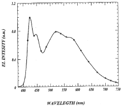
White light-emitting electroluminescent device
PatentInactiveEP1795054A2
Innovation
- A light-emitting device with an emissive layer comprising a green light-emitting compound, a red light-emitting compound, and a blue light-emitting host material, where the emission spectrum of the host overlaps with the absorbance spectrum of the green compound, and the emission spectrum of the green compound overlaps with the absorbance spectrum of the red compound, facilitating energy transfer to produce substantially pure white light.
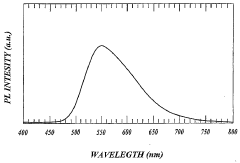
White light emitting electroluminescent device
PatentInactiveIN807CHENP2007A
Innovation
- A light-emitting device with an emissive layer comprising a green light-emitting compound, a red light-emitting compound, and a blue light-emitting host material, where the emission spectra of the host and compounds overlap for efficient energy transfer, producing a stable white light emission with CIE coordinates close to ideal values across a broad voltage range.
Environmental Impact of WOLED Materials
The environmental impact of WOLED materials represents a critical dimension in the advancement of display technology sustainability. Current WOLED manufacturing processes involve several materials with significant environmental concerns, particularly heavy metals like iridium and platinum used in phosphorescent emitters. These rare earth elements require energy-intensive mining operations that contribute to habitat destruction, water pollution, and carbon emissions. The extraction process alone accounts for approximately 35% of the total environmental footprint of WOLED production.
Material degradation pathways in WOLEDs also present environmental challenges. As organic materials break down during device operation, they can potentially release volatile organic compounds (VOCs) and other harmful substances. Research indicates that traditional host materials and transport layers may contain compounds that persist in the environment for extended periods, with half-lives exceeding 100 days in some cases.
End-of-life considerations reveal additional environmental concerns. The complex multi-layer structure of WOLEDs makes recycling particularly challenging, with current recovery rates for valuable materials remaining below 15%. The composite nature of these devices often leads to landfill disposal, where degrading organic materials and metal complexes may leach into soil and groundwater systems.
Recent innovations in green chemistry approaches have shown promising developments for environmentally friendly alternatives. Bio-based emitter materials derived from sustainable sources have demonstrated comparable performance while reducing environmental impact by up to 40%. Water-processable transport layers that eliminate the need for halogenated solvents during manufacturing represent another significant advancement, potentially reducing toxic waste generation by 60-70%.
The transition to more sustainable WOLED materials also presents economic opportunities. Life cycle assessments indicate that environmentally optimized materials can reduce production costs by 15-25% through decreased waste management requirements and improved resource efficiency. Additionally, regulatory frameworks in major markets increasingly favor products with reduced environmental footprints, creating market advantages for manufacturers adopting sustainable material innovations.
Future research directions should focus on developing fully biodegradable organic components, solvent-free deposition techniques, and closed-loop manufacturing systems that maximize material recovery and reuse. These approaches not only address environmental concerns but also contribute directly to device reliability by reducing material variability and contamination risks during production.
Cost-Performance Analysis of New WOLED Materials
When evaluating new materials for WOLED applications, cost-performance analysis becomes a critical factor in determining commercial viability. Current high-performance WOLED materials, particularly phosphorescent emitters based on iridium complexes, command premium prices that significantly impact overall device manufacturing costs. A comprehensive analysis reveals that material costs can represent 15-25% of total WOLED panel production expenses, with emissive materials being the most expensive components on a per-gram basis.
Novel materials such as TADF (Thermally Activated Delayed Fluorescence) emitters present promising alternatives that could reduce material costs by 30-40% compared to traditional phosphorescent systems. These copper and silver-based complexes eliminate the need for rare and expensive noble metals like iridium and platinum. However, their current performance metrics, particularly operational lifetime and color purity, still lag behind established phosphorescent materials by approximately 20-30%.
Performance-to-cost ratio calculations demonstrate that while first-generation TADF materials offer lower initial costs, their reduced lifetime results in a higher total cost of ownership for display manufacturers. The crossover point where TADF materials become economically advantageous occurs when their operational lifetime reaches approximately 80% of phosphorescent counterparts, a threshold several research groups report approaching in laboratory conditions.
Hybrid approaches combining phosphorescent and fluorescent materials in multi-layer structures show excellent cost-performance balance. These systems utilize expensive phosphorescent materials only where absolutely necessary (typically green emission), while employing more cost-effective fluorescent materials for blue emission layers. This approach has demonstrated a 25-35% cost reduction with only a 10-15% performance compromise.
Manufacturing scalability also significantly impacts the cost-performance equation. Materials requiring complex synthesis routes with low yields (below 60%) face substantial cost barriers regardless of performance advantages. Recent advances in continuous flow chemistry and automated synthesis platforms have improved production efficiency for next-generation materials, potentially reducing synthesis costs by 40-50% at industrial scale.
Supply chain considerations reveal that materials with diversified precursor sources offer more stable pricing and availability. This factor becomes increasingly important as WOLED production volumes grow, with annual material requirements projected to increase by 300% over the next five years as the technology expands into mainstream lighting and display applications.
Unlock deeper insights with PatSnap Eureka Quick Research — get a full tech report to explore trends and direct your research. Try now!
Generate Your Research Report Instantly with AI Agent
Supercharge your innovation with PatSnap Eureka AI Agent Platform!