

How to Increase WOLED Pixel Density Without Sacrificing Power
SEP 15, 20259 MIN READ
Generate Your Research Report Instantly with AI Agent
PatSnap Eureka helps you evaluate technical feasibility & market potential.
WOLED Pixel Density Evolution and Objectives
White Organic Light-Emitting Diode (WOLED) technology has undergone significant evolution since its inception in the early 1990s. Initially characterized by low efficiency and limited lifespan, WOLED displays have transformed into high-performance solutions for various applications including smartphones, televisions, and wearable devices. The pixel density of WOLED displays has been a critical factor in this evolution, progressing from early implementations with densities below 100 pixels per inch (PPI) to current high-end displays exceeding 500 PPI in premium smartphones and VR headsets.
The technological trajectory of WOLED pixel density improvement has been marked by several breakthrough innovations. The transition from passive-matrix to active-matrix driving schemes in the early 2000s enabled significant increases in resolution while maintaining power efficiency. Subsequently, the development of top-emission structures, microcavity designs, and advanced thin-film encapsulation techniques further facilitated pixel miniaturization without compromising luminous efficacy.
Current industry objectives for WOLED pixel density enhancement are primarily driven by emerging applications in augmented reality (AR), virtual reality (VR), and ultra-high-definition displays. These applications demand pixel densities exceeding 1000 PPI while maintaining or improving power efficiency. The technical challenge lies in the fundamental trade-off between pixel size and light output – as pixel dimensions decrease, the active emission area typically shrinks, requiring higher current densities to maintain brightness, which in turn reduces efficiency and device lifetime.
The strategic goals for WOLED pixel density advancement can be categorized into three primary objectives. First, achieving ultra-high resolution (>1500 PPI) for near-eye display applications while maintaining acceptable power consumption levels below 2W. Second, developing scalable manufacturing processes capable of producing high-density WOLED panels with yields exceeding 80% at commercially viable costs. Third, ensuring that increased pixel density does not compromise other critical performance parameters such as color gamut, viewing angle, and operational lifetime.
Looking forward, the roadmap for WOLED pixel density evolution aims to reach 2000-3000 PPI by 2025-2027, enabling truly immersive AR/VR experiences without the "screen door effect" that currently plagues many head-mounted displays. This ambitious target necessitates fundamental innovations in materials science, device architecture, and manufacturing processes to overcome the current power-density limitations.
The technological trajectory of WOLED pixel density improvement has been marked by several breakthrough innovations. The transition from passive-matrix to active-matrix driving schemes in the early 2000s enabled significant increases in resolution while maintaining power efficiency. Subsequently, the development of top-emission structures, microcavity designs, and advanced thin-film encapsulation techniques further facilitated pixel miniaturization without compromising luminous efficacy.
Current industry objectives for WOLED pixel density enhancement are primarily driven by emerging applications in augmented reality (AR), virtual reality (VR), and ultra-high-definition displays. These applications demand pixel densities exceeding 1000 PPI while maintaining or improving power efficiency. The technical challenge lies in the fundamental trade-off between pixel size and light output – as pixel dimensions decrease, the active emission area typically shrinks, requiring higher current densities to maintain brightness, which in turn reduces efficiency and device lifetime.
The strategic goals for WOLED pixel density advancement can be categorized into three primary objectives. First, achieving ultra-high resolution (>1500 PPI) for near-eye display applications while maintaining acceptable power consumption levels below 2W. Second, developing scalable manufacturing processes capable of producing high-density WOLED panels with yields exceeding 80% at commercially viable costs. Third, ensuring that increased pixel density does not compromise other critical performance parameters such as color gamut, viewing angle, and operational lifetime.
Looking forward, the roadmap for WOLED pixel density evolution aims to reach 2000-3000 PPI by 2025-2027, enabling truly immersive AR/VR experiences without the "screen door effect" that currently plagues many head-mounted displays. This ambitious target necessitates fundamental innovations in materials science, device architecture, and manufacturing processes to overcome the current power-density limitations.
Market Demand for High-Resolution WOLED Displays
The global market for high-resolution WOLED (White Organic Light-Emitting Diode) displays has experienced exponential growth over the past five years, driven primarily by increasing consumer demand for premium visual experiences across multiple device categories. Market research indicates that the WOLED display segment is projected to grow at a compound annual growth rate of 21.3% through 2028, significantly outpacing traditional display technologies.
Consumer electronics manufacturers are facing intensifying pressure to deliver devices with higher pixel densities as users become more discerning about display quality. Particularly in the smartphone and wearable segments, where devices are viewed at close proximity, the demand for pixel densities exceeding 500 PPI (pixels per inch) has become standard, with premium devices pushing beyond 1000 PPI. This trend is evidenced by recent flagship smartphone releases where display quality has become a primary differentiating factor.
The virtual reality and augmented reality markets represent another significant driver for high-resolution WOLED development. These applications require extremely high pixel densities to eliminate the "screen door effect" and create truly immersive experiences. Industry analysts note that VR headset manufacturers are targeting minimum resolutions of 2000×2000 pixels per eye, necessitating WOLED displays with exceptional pixel density while maintaining power efficiency.
Professional markets, including medical imaging, design, and content creation, are increasingly adopting WOLED technology due to its superior color accuracy and contrast ratios. These sectors demand displays with resolutions that can accurately represent minute details without distortion, creating a specialized high-value market segment for ultra-high-resolution WOLED panels.
The automotive industry represents an emerging market for high-resolution WOLED displays, with premium vehicle manufacturers incorporating increasingly sophisticated dashboard and entertainment systems. This sector values WOLED's ability to deliver high visibility across varying lighting conditions while maintaining power efficiency, particularly important in electric vehicles where power management is critical.
Consumer preference surveys indicate that display quality ranks among the top three purchasing considerations for smartphones, tablets, and televisions. However, these same surveys reveal that battery life remains the number one concern, creating a challenging balance for manufacturers seeking to increase resolution without compromising device longevity.
Market analysis reveals a significant price premium for devices featuring higher-resolution WOLED displays, with consumers demonstrating willingness to pay up to 30% more for superior visual experiences. This price elasticity provides manufacturers with economic incentive to solve the technical challenges associated with increasing pixel density while maintaining acceptable power consumption levels.
Consumer electronics manufacturers are facing intensifying pressure to deliver devices with higher pixel densities as users become more discerning about display quality. Particularly in the smartphone and wearable segments, where devices are viewed at close proximity, the demand for pixel densities exceeding 500 PPI (pixels per inch) has become standard, with premium devices pushing beyond 1000 PPI. This trend is evidenced by recent flagship smartphone releases where display quality has become a primary differentiating factor.
The virtual reality and augmented reality markets represent another significant driver for high-resolution WOLED development. These applications require extremely high pixel densities to eliminate the "screen door effect" and create truly immersive experiences. Industry analysts note that VR headset manufacturers are targeting minimum resolutions of 2000×2000 pixels per eye, necessitating WOLED displays with exceptional pixel density while maintaining power efficiency.
Professional markets, including medical imaging, design, and content creation, are increasingly adopting WOLED technology due to its superior color accuracy and contrast ratios. These sectors demand displays with resolutions that can accurately represent minute details without distortion, creating a specialized high-value market segment for ultra-high-resolution WOLED panels.
The automotive industry represents an emerging market for high-resolution WOLED displays, with premium vehicle manufacturers incorporating increasingly sophisticated dashboard and entertainment systems. This sector values WOLED's ability to deliver high visibility across varying lighting conditions while maintaining power efficiency, particularly important in electric vehicles where power management is critical.
Consumer preference surveys indicate that display quality ranks among the top three purchasing considerations for smartphones, tablets, and televisions. However, these same surveys reveal that battery life remains the number one concern, creating a challenging balance for manufacturers seeking to increase resolution without compromising device longevity.
Market analysis reveals a significant price premium for devices featuring higher-resolution WOLED displays, with consumers demonstrating willingness to pay up to 30% more for superior visual experiences. This price elasticity provides manufacturers with economic incentive to solve the technical challenges associated with increasing pixel density while maintaining acceptable power consumption levels.
Technical Barriers in High-Density WOLED Implementation
Despite significant advancements in WOLED technology, several technical barriers impede the implementation of high-density WOLED displays without compromising power efficiency. The fundamental challenge stems from the inverse relationship between pixel density and power efficiency. As pixels become smaller to increase density, the light-emitting area decreases proportionally, requiring higher current densities to maintain brightness levels, which accelerates device degradation and reduces operational lifespan.
Material limitations present another significant barrier. Current organic emitter materials exhibit efficiency roll-off at high current densities, a phenomenon known as efficiency droop. This non-linear decrease in quantum efficiency at higher brightness levels becomes particularly problematic in high-density displays where smaller pixels must operate at elevated current densities to maintain luminance standards.
Thermal management emerges as a critical challenge in high-density WOLED implementations. Smaller pixels operating at higher current densities generate more heat per unit area, creating thermal hotspots that accelerate material degradation and color shift. Conventional thermal management solutions add bulk and complexity, contradicting the miniaturization goals of high-density displays.
Manufacturing precision requirements escalate exponentially with increased pixel density. The fabrication of smaller WOLED pixels demands unprecedented precision in deposition processes, with alignment tolerances measured in nanometers rather than micrometers. Current industrial-scale manufacturing equipment struggles to consistently achieve these precision levels, resulting in yield issues and increased production costs.
Optical efficiency challenges become more pronounced at higher pixel densities. Light extraction from smaller pixels suffers from increased internal reflection and waveguiding effects. Additionally, the proportionally larger non-emissive areas between pixels (bezels) in high-density displays reduce the overall aperture ratio, necessitating higher pixel brightness to maintain perceived display luminance.
Driving circuit complexity increases substantially with pixel density. The integration of TFT backplanes with sufficient current-handling capabilities while maintaining small footprints presents significant design challenges. Higher resolution displays require more complex addressing schemes and faster refresh rates, increasing power consumption in the driving electronics and partially offsetting efficiency gains in the WOLED elements themselves.
Color management becomes increasingly difficult as pixel size decreases. Maintaining color accuracy and consistency across smaller sub-pixels requires more precise deposition of organic materials and more sophisticated color filters, which can reduce overall light transmission and necessitate higher power to compensate.
Material limitations present another significant barrier. Current organic emitter materials exhibit efficiency roll-off at high current densities, a phenomenon known as efficiency droop. This non-linear decrease in quantum efficiency at higher brightness levels becomes particularly problematic in high-density displays where smaller pixels must operate at elevated current densities to maintain luminance standards.
Thermal management emerges as a critical challenge in high-density WOLED implementations. Smaller pixels operating at higher current densities generate more heat per unit area, creating thermal hotspots that accelerate material degradation and color shift. Conventional thermal management solutions add bulk and complexity, contradicting the miniaturization goals of high-density displays.
Manufacturing precision requirements escalate exponentially with increased pixel density. The fabrication of smaller WOLED pixels demands unprecedented precision in deposition processes, with alignment tolerances measured in nanometers rather than micrometers. Current industrial-scale manufacturing equipment struggles to consistently achieve these precision levels, resulting in yield issues and increased production costs.
Optical efficiency challenges become more pronounced at higher pixel densities. Light extraction from smaller pixels suffers from increased internal reflection and waveguiding effects. Additionally, the proportionally larger non-emissive areas between pixels (bezels) in high-density displays reduce the overall aperture ratio, necessitating higher pixel brightness to maintain perceived display luminance.
Driving circuit complexity increases substantially with pixel density. The integration of TFT backplanes with sufficient current-handling capabilities while maintaining small footprints presents significant design challenges. Higher resolution displays require more complex addressing schemes and faster refresh rates, increasing power consumption in the driving electronics and partially offsetting efficiency gains in the WOLED elements themselves.
Color management becomes increasingly difficult as pixel size decreases. Maintaining color accuracy and consistency across smaller sub-pixels requires more precise deposition of organic materials and more sophisticated color filters, which can reduce overall light transmission and necessitate higher power to compensate.
Current Approaches to WOLED Pixel Density Enhancement
01 WOLED pixel structure and arrangement for high density displays
White Organic Light-Emitting Diode (WOLED) displays can achieve higher pixel densities through optimized pixel structures and arrangements. These designs include stacked RGB emitting layers, tandem structures, and micro-cavity designs that allow for more efficient use of display area. Advanced pixel arrangements like pentile or diamond patterns can further increase the effective resolution while maintaining color accuracy and brightness in high-density displays.- WOLED pixel structure and arrangement for high density displays: White organic light-emitting diode (WOLED) displays can achieve higher pixel densities through optimized pixel structures and arrangements. These designs include stacked RGB organic layers that emit white light, which can be filtered to produce different colors. Advanced pixel arrangements like pentile or diamond patterns allow for higher effective resolution while maintaining color accuracy. These structures enable displays with higher pixel densities suitable for high-resolution applications like VR/AR headsets and mobile devices.
- Color filter integration with WOLED for enhanced pixel density: Integrating color filters with WOLED technology enables higher pixel densities while maintaining color accuracy. By using a single white light source with RGB color filters, manufacturers can create displays with smaller pixel sizes compared to traditional RGB OLED structures. This approach simplifies the manufacturing process and allows for higher resolution displays. The color filter design and placement are optimized to minimize light loss while maximizing color purity, contributing to improved pixel density in WOLED displays.
- Tandem WOLED structures for improved efficiency at high pixel densities: Tandem WOLED structures stack multiple emitting units vertically to improve efficiency and lifetime at high pixel densities. These multi-unit structures allow for increased brightness without increasing current density, which is crucial for high-resolution displays. By connecting multiple OLED units in series with charge generation layers between them, manufacturers can achieve higher luminance while maintaining the small pixel size needed for high-density displays. This approach helps overcome efficiency limitations that typically occur when pixel sizes are reduced.
- Microcavity effects for enhanced WOLED pixel performance: Microcavity effects can be utilized in WOLED displays to enhance pixel performance at high densities. By carefully designing the optical cavity between reflective electrodes, light emission can be tuned and enhanced at specific wavelengths. This approach improves color purity and increases the external quantum efficiency of the device, allowing for smaller pixels while maintaining brightness and color quality. Microcavity-enhanced WOLEDs can achieve higher pixel densities with improved optical characteristics compared to conventional structures.
- Advanced driving schemes for high-density WOLED displays: Advanced driving schemes are essential for operating high-density WOLED displays efficiently. These include compensation circuits that address non-uniformity issues that become more pronounced at higher pixel densities. Time-division and pulse-width modulation techniques enable precise control of brightness levels in densely packed pixels. Additionally, specialized thin-film transistor (TFT) backplane designs with higher mobility and smaller feature sizes support the increased pixel density requirements of WOLED displays while maintaining image quality and reducing power consumption.
02 Color filter integration with WOLED for enhanced pixel density
Integrating color filters with WOLED technology enables higher pixel densities by allowing a single white light source to produce multiple colors through filtering. This approach eliminates the need for separate RGB sub-pixels, reducing the overall pixel footprint. Advanced color filter materials and arrangements can optimize color gamut while maintaining high resolution. The combination of WOLED with precisely aligned color filters enables displays with superior pixel density for applications requiring high-resolution imagery.Expand Specific Solutions03 Thin-film transistor (TFT) backplane designs for high-density WOLED displays
Specialized TFT backplane designs are crucial for achieving high pixel densities in WOLED displays. These include oxide semiconductor TFTs, low-temperature polysilicon (LTPS) TFTs, and advanced circuit layouts that minimize the transistor footprint while maintaining driving capabilities. Stacked or vertically integrated TFT structures can further reduce the horizontal space requirements, allowing for more pixels per inch. These backplane technologies enable the creation of ultra-high-resolution WOLED displays for applications like VR/AR headsets and professional monitors.Expand Specific Solutions04 Manufacturing techniques for high-density WOLED panels
Advanced manufacturing techniques are essential for producing high-density WOLED displays. These include fine metal mask (FMM) deposition, inkjet printing of organic materials, laser patterning, and photolithography processes adapted for OLED materials. Precision alignment systems ensure accurate positioning of sub-pixels and color filters. Novel encapsulation methods protect the organic materials while maintaining the thin profile necessary for high pixel density. These manufacturing innovations enable mass production of displays with increasingly higher resolutions.Expand Specific Solutions05 Optical enhancement technologies for WOLED pixel density
Optical enhancement technologies can effectively increase the perceived pixel density of WOLED displays without physically increasing the number of pixels. These include micro-lens arrays that focus light, optical waveguides that direct emission, and light extraction structures that improve efficiency. Quantum dot enhancement films can narrow the emission spectrum of white light, resulting in purer colors after filtering. Anti-reflection coatings and polarization technologies further improve the visual clarity and apparent resolution of high-density WOLED displays.Expand Specific Solutions
Leading WOLED Display Manufacturers and Competitors
The WOLED pixel density enhancement market is currently in a growth phase, with increasing demand for high-resolution displays that maintain power efficiency. The global market size for advanced OLED technologies is expanding rapidly, driven by consumer electronics and premium display applications. Leading players like Samsung Display and BOE Technology are at the forefront of technological innovation, with Samsung demonstrating mature WOLED technologies and BOE investing heavily in next-generation solutions. Other significant competitors include LG Display (through Global OLED Technology), TCL China Star, and Apple, who are advancing pixel architecture designs that optimize light emission while managing power consumption. The technology remains in mid-maturity phase, with ongoing R&D focused on materials science and micro-circuit design to overcome the traditional trade-off between pixel density and power requirements.
BOE Technology Group Co., Ltd.
Technical Solution: BOE has developed a novel approach to WOLED pixel density enhancement through their advanced oxide backplane technology. Their solution incorporates high-mobility oxide TFT arrays that enable smaller pixel circuits while maintaining driving capabilities. BOE's technology utilizes a specialized tandem WOLED structure with optimized charge generation layers that effectively doubles the current efficiency without proportional power increase. The company has implemented micro-lens array (MLA) technology on the emission side to improve light extraction efficiency by approximately 20%, allowing for smaller pixels without brightness loss. BOE's pixel circuit design incorporates advanced compensation algorithms that minimize power consumption during high-resolution operation. Additionally, they've developed specialized color filter arrangements that maximize color gamut while minimizing optical losses in high-density displays.
Strengths: Strong manufacturing capacity and scale; vertical integration from backplanes to module assembly; competitive cost structure for mass production; growing IP portfolio in oxide TFT technology. Weaknesses: Still catching up to Korean manufacturers in ultimate OLED performance metrics; challenges with yield rates for the highest density displays; relatively newer entrant to premium WOLED market compared to competitors.
Samsung Display Co., Ltd.
Technical Solution: Samsung has developed advanced WOLED pixel architectures that utilize micro-cavity structures to enhance light extraction efficiency. Their approach involves optimizing the OLED stack with precisely controlled emission layer thicknesses and implementing multi-unit stacking technology. Samsung's solution incorporates quantum dot color filters (QD-OLED) that allow for higher pixel densities while maintaining power efficiency. The company has implemented advanced thin-film encapsulation (TFE) techniques that reduce the overall thickness of the display stack, enabling higher pixel densities. Additionally, Samsung utilizes advanced driving schemes with optimized transistor designs that reduce power consumption during high-resolution operation. Their latest developments include pixel circuit innovations that compensate for threshold voltage variations, ensuring uniform brightness across high-density displays.
Strengths: Industry-leading expertise in OLED manufacturing at scale; proprietary QD-OLED technology provides superior color volume while maintaining efficiency; extensive IP portfolio in display technologies. Weaknesses: Higher manufacturing costs compared to conventional LCD; complex fabrication processes requiring significant capital investment; challenges with blue OLED material lifetime in high-density applications.
Key Patents in Power-Efficient WOLED Pixel Architecture
White organic light-emitting diode
PatentActiveTW201134288A
Innovation
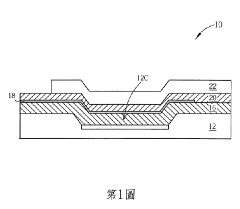
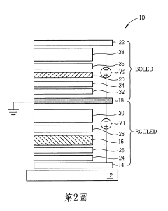
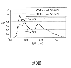
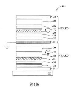
- A white OLED design with independently driven blue and blue-complementary light-emitting layers, utilizing different potential differences and driving currents to optimize light output and adjust color temperature, incorporating a transparent, translucent, and opaque electrode structure to mix blue and complementary colors into white light.
Organic light emitting diode display power management based on usage scaling
PatentActiveUS11011109B1
Innovation
- The system divides the OLED display into zones with adjustable pixel density, refresh rate, and brightness to manage power and thermal constraints, using a display zone manager to optimize pixel settings based on detected conditions, and employs a compensation table validated by camera images to ensure accurate visual image representation without ghosting.


Material Science Innovations for WOLED Efficiency
Recent advancements in material science have opened promising pathways for enhancing WOLED efficiency without compromising pixel density or power consumption. Novel emitter materials, particularly phosphorescent and thermally activated delayed fluorescence (TADF) compounds, demonstrate quantum efficiencies approaching 100%, significantly outperforming traditional fluorescent materials limited to 25% efficiency. These materials effectively convert electrical energy into light with minimal heat loss, addressing a fundamental challenge in WOLED technology.
Nanostructured electrode materials represent another breakthrough area, with transparent conductive oxides (TCOs) being engineered at the nanoscale to improve both conductivity and transparency. Indium tin oxide (ITO) alternatives such as silver nanowire networks and graphene-based composites offer superior performance characteristics while potentially reducing manufacturing costs. These materials enable more efficient current distribution across the WOLED panel while maintaining optical clarity.
Host-guest systems optimization has yielded significant efficiency gains through improved energy transfer mechanisms. By carefully engineering the energy levels between host materials and emitter dopants, researchers have achieved more efficient exciton formation and energy transfer. Multi-component host systems that incorporate both electron and hole transport capabilities have demonstrated particular promise in balancing charge transport and recombination efficiency.
Charge transport layer innovations focus on developing materials with higher mobility and more balanced electron/hole transport. Novel small-molecule and polymer-based transport materials with optimized energy levels facilitate more efficient charge injection and transport through the device structure. These materials reduce operating voltage requirements while maintaining brightness levels, directly addressing power efficiency concerns at higher pixel densities.
Optical management strategies through advanced light extraction techniques have emerged as a critical efficiency enhancement approach. Micro-lens arrays, photonic crystals, and nanostructured outcoupling layers can significantly reduce waveguiding losses within the device structure. These techniques can potentially increase external quantum efficiency by 30-50% without modifying the active emissive materials, effectively extracting light that would otherwise be trapped within the device.
Barrier and encapsulation materials have evolved to provide superior protection against moisture and oxygen while maintaining flexibility and transparency. Atomic layer deposition techniques enable ultra-thin barrier films with exceptional barrier properties, while new composite materials offer self-healing capabilities to extend device lifetimes. These advancements ensure that efficiency gains are maintained throughout the operational lifetime of high-density WOLED displays.
Nanostructured electrode materials represent another breakthrough area, with transparent conductive oxides (TCOs) being engineered at the nanoscale to improve both conductivity and transparency. Indium tin oxide (ITO) alternatives such as silver nanowire networks and graphene-based composites offer superior performance characteristics while potentially reducing manufacturing costs. These materials enable more efficient current distribution across the WOLED panel while maintaining optical clarity.
Host-guest systems optimization has yielded significant efficiency gains through improved energy transfer mechanisms. By carefully engineering the energy levels between host materials and emitter dopants, researchers have achieved more efficient exciton formation and energy transfer. Multi-component host systems that incorporate both electron and hole transport capabilities have demonstrated particular promise in balancing charge transport and recombination efficiency.
Charge transport layer innovations focus on developing materials with higher mobility and more balanced electron/hole transport. Novel small-molecule and polymer-based transport materials with optimized energy levels facilitate more efficient charge injection and transport through the device structure. These materials reduce operating voltage requirements while maintaining brightness levels, directly addressing power efficiency concerns at higher pixel densities.
Optical management strategies through advanced light extraction techniques have emerged as a critical efficiency enhancement approach. Micro-lens arrays, photonic crystals, and nanostructured outcoupling layers can significantly reduce waveguiding losses within the device structure. These techniques can potentially increase external quantum efficiency by 30-50% without modifying the active emissive materials, effectively extracting light that would otherwise be trapped within the device.
Barrier and encapsulation materials have evolved to provide superior protection against moisture and oxygen while maintaining flexibility and transparency. Atomic layer deposition techniques enable ultra-thin barrier films with exceptional barrier properties, while new composite materials offer self-healing capabilities to extend device lifetimes. These advancements ensure that efficiency gains are maintained throughout the operational lifetime of high-density WOLED displays.
Thermal Management Solutions for High-Density WOLED
Effective thermal management is critical for high-density WOLED displays, as increased pixel density inevitably leads to greater heat generation within a confined space. The thermal challenges are particularly pronounced when maintaining power efficiency while increasing resolution, as heat accumulation can significantly degrade WOLED materials, reduce operational lifespan, and compromise display performance.
Current thermal management approaches for high-density WOLEDs include advanced heat sink designs that efficiently dissipate heat away from the pixel array. These solutions often incorporate materials with superior thermal conductivity such as graphene-enhanced composites or metal-matrix materials that can transfer heat up to 10 times more effectively than traditional options while maintaining minimal thickness requirements for modern display designs.
Active cooling systems represent another frontier in thermal management, with microscale heat pipes and vapor chambers being integrated into display assemblies. These systems can transport heat from high-temperature regions to designated cooling areas with minimal thermal resistance. Some cutting-edge designs incorporate thermoelectric cooling elements strategically positioned to address hotspots that typically develop in high-brightness regions of WOLED displays.
Thermal interface materials (TIMs) have also evolved significantly, with new formulations offering thermal conductivity values exceeding 20 W/m·K while maintaining the flexibility needed for display applications. These advanced TIMs ensure efficient heat transfer between components and cooling structures without adding substantial thickness to the display stack.
Computational fluid dynamics (CFD) modeling has become instrumental in optimizing thermal management solutions before physical prototyping. These simulation tools allow engineers to predict heat distribution patterns and identify potential thermal bottlenecks in high-density WOLED designs, enabling more targeted cooling solutions that address specific thermal challenges without overengineering the entire system.
Emerging approaches include dynamic thermal management systems that adjust cooling intensity based on real-time temperature monitoring. These systems incorporate microscale temperature sensors distributed throughout the display panel, coupled with variable-performance cooling elements that activate only when and where needed, thus optimizing power consumption while maintaining safe operating temperatures.
The integration of thermal management considerations into the earliest stages of WOLED panel design has proven particularly effective. By adopting thermal-aware layout strategies that distribute heat-generating elements more evenly and incorporating dedicated thermal channels within the panel structure, manufacturers can achieve higher pixel densities without requiring disproportionately powerful cooling solutions.
Current thermal management approaches for high-density WOLEDs include advanced heat sink designs that efficiently dissipate heat away from the pixel array. These solutions often incorporate materials with superior thermal conductivity such as graphene-enhanced composites or metal-matrix materials that can transfer heat up to 10 times more effectively than traditional options while maintaining minimal thickness requirements for modern display designs.
Active cooling systems represent another frontier in thermal management, with microscale heat pipes and vapor chambers being integrated into display assemblies. These systems can transport heat from high-temperature regions to designated cooling areas with minimal thermal resistance. Some cutting-edge designs incorporate thermoelectric cooling elements strategically positioned to address hotspots that typically develop in high-brightness regions of WOLED displays.
Thermal interface materials (TIMs) have also evolved significantly, with new formulations offering thermal conductivity values exceeding 20 W/m·K while maintaining the flexibility needed for display applications. These advanced TIMs ensure efficient heat transfer between components and cooling structures without adding substantial thickness to the display stack.
Computational fluid dynamics (CFD) modeling has become instrumental in optimizing thermal management solutions before physical prototyping. These simulation tools allow engineers to predict heat distribution patterns and identify potential thermal bottlenecks in high-density WOLED designs, enabling more targeted cooling solutions that address specific thermal challenges without overengineering the entire system.
Emerging approaches include dynamic thermal management systems that adjust cooling intensity based on real-time temperature monitoring. These systems incorporate microscale temperature sensors distributed throughout the display panel, coupled with variable-performance cooling elements that activate only when and where needed, thus optimizing power consumption while maintaining safe operating temperatures.
The integration of thermal management considerations into the earliest stages of WOLED panel design has proven particularly effective. By adopting thermal-aware layout strategies that distribute heat-generating elements more evenly and incorporating dedicated thermal channels within the panel structure, manufacturers can achieve higher pixel densities without requiring disproportionately powerful cooling solutions.
Unlock deeper insights with PatSnap Eureka Quick Research — get a full tech report to explore trends and direct your research. Try now!
Generate Your Research Report Instantly with AI Agent
Supercharge your innovation with PatSnap Eureka AI Agent Platform!