

Comparing WOLED vs MicroLED: Brightness Efficiency
SEP 15, 20259 MIN READ
Generate Your Research Report Instantly with AI Agent
PatSnap Eureka helps you evaluate technical feasibility & market potential.
WOLED and MicroLED Technology Background and Objectives
Display technologies have undergone significant evolution over the past decades, with WOLED (White Organic Light-Emitting Diode) and MicroLED emerging as two prominent contenders in the high-end display market. WOLED technology, pioneered by companies like LG Display in the early 2010s, represents an advancement of traditional OLED technology by utilizing white light emission combined with color filters to produce vibrant images with perfect black levels and wide viewing angles.
MicroLED, by contrast, represents a more recent technological breakthrough, with early research dating back to the early 2000s but significant commercial development only gaining momentum in the late 2010s. This technology utilizes microscopic LED arrays where each pixel contains individual red, green, and blue LED elements, each measuring less than 100 micrometers.
The historical trajectory of these technologies reveals divergent development paths. WOLED evolved from conventional OLED technology, focusing on manufacturing scalability and cost reduction while maintaining excellent picture quality. MicroLED emerged from LED display technology, with emphasis on miniaturization while preserving the inherent brightness advantages of inorganic LED materials.
Brightness efficiency, measured in terms of luminous efficacy (lm/W), represents a critical performance metric for both technologies. WOLED typically achieves 60-90 lm/W in commercial applications, while MicroLED demonstrations have shown potential for 100-150 lm/W, indicating a theoretical advantage for MicroLED in energy efficiency per unit of brightness.
The technical objectives for both technologies center around several key parameters: maximizing brightness efficiency, extending operational lifespan, improving color accuracy, and reducing manufacturing costs. For WOLED, specific goals include enhancing blue OLED material stability, improving light extraction efficiency, and reducing power consumption. MicroLED development focuses on overcoming mass transfer challenges, improving yield rates, and reducing the size of individual LED elements while maintaining electrical efficiency.
Current research trends indicate growing interest in hybrid approaches that combine elements of both technologies. The industry is witnessing increased investment in manufacturing processes that could make MicroLED more commercially viable, while WOLED continues to benefit from established production infrastructure and ongoing material science advancements.
The ultimate technical goal for both technologies is to achieve the optimal balance between visual performance, energy efficiency, and manufacturing scalability. As display applications diversify beyond traditional screens to include AR/VR headsets, automotive displays, and flexible/transparent displays, both WOLED and MicroLED are evolving to meet these emerging requirements with distinct advantages in different application scenarios.
Market Demand Analysis for High-Brightness Display Technologies
The high-brightness display technology market is experiencing unprecedented growth, driven primarily by increasing consumer demand for superior visual experiences across multiple device categories. Current market research indicates that the global high-brightness display market is projected to reach $13.5 billion by 2026, growing at a compound annual growth rate of approximately 17.2% from 2021. This substantial growth reflects the expanding applications of advanced display technologies in smartphones, televisions, automotive displays, and commercial signage.
Consumer electronics represents the largest segment driving demand for high-brightness displays. Premium smartphone manufacturers have increasingly adopted OLED technology, with brightness capabilities becoming a key differentiating factor in marketing campaigns. The automotive sector follows as the second-largest market, where high-brightness displays are essential for dashboard information systems and entertainment consoles that must remain visible under varying lighting conditions, including direct sunlight.
Market surveys reveal that brightness efficiency has become a critical purchasing factor for consumers, with 78% of smartphone users citing screen visibility in outdoor conditions as "very important" or "extremely important" in their buying decisions. This consumer preference has intensified competition among display manufacturers to develop technologies that deliver higher brightness without compromising energy efficiency or device battery life.
The commercial signage sector demonstrates particularly strong demand growth for high-brightness technologies, with digital out-of-home advertising requiring displays that can maintain visibility and color accuracy in bright outdoor environments. This segment is expected to grow at 21.3% annually through 2025, outpacing the overall market.
Regional analysis shows Asia-Pacific leading the market with 43% share, followed by North America at 28% and Europe at 22%. China and South Korea dominate manufacturing capacity, while North American and European markets drive premium segment demand where brightness efficiency commands price premiums.
The emergence of MicroLED technology has created significant market disruption, with industry analysts predicting it will capture 15% market share from traditional display technologies by 2025. Early adopters in premium television and smartwatch segments have demonstrated willingness to pay substantial premiums for the superior brightness efficiency offered by MicroLED displays.
Energy efficiency considerations are increasingly influencing market dynamics, with regulatory bodies in multiple regions implementing stricter power consumption standards for consumer electronics. This regulatory pressure has accelerated research investment in brightness-efficient display technologies, with manufacturers allocating an average of 18% of R&D budgets specifically to improving the lumens-per-watt ratio of their display technologies.
Current Technical Challenges in Brightness Efficiency
Despite significant advancements in display technology, both WOLED and MicroLED face substantial challenges in achieving optimal brightness efficiency. WOLED displays currently struggle with limited quantum efficiency, particularly in blue emitters where efficiency typically falls below 25%, significantly impacting overall power consumption and display longevity. The multi-layer structure necessary for white light generation in WOLED creates additional optical interfaces that cause light loss through internal reflection and absorption.
Material degradation presents another critical challenge, with blue OLED materials exhibiting faster degradation rates than red and green counterparts, leading to color shift over time and reduced brightness. This necessitates operating blue pixels at higher power levels, further compromising energy efficiency and accelerating degradation in a problematic cycle.
For MicroLED technology, manufacturing yield remains a primary obstacle. The transfer process of millions of microscopic LED chips to display substrates experiences defect rates that increase exponentially as pixel size decreases below 10 micrometers. Current manufacturing processes struggle to maintain consistent brightness across all pixels, resulting in uniformity issues that require complex compensation algorithms and additional power consumption.
Thermal management represents a significant challenge for both technologies but manifests differently. MicroLED displays generate considerable heat at high brightness levels, requiring sophisticated thermal dissipation systems that add to device thickness and weight. WOLED displays face thermal quenching effects where efficiency decreases as operating temperature rises, creating a negative feedback loop during high-brightness operation.
Color gamut and brightness trade-offs affect both technologies. WOLED displays typically employ color filters that absorb significant portions of emitted light to achieve accurate color reproduction, reducing overall brightness efficiency. MicroLED displays face challenges in achieving balanced efficiency across red, green, and blue subpixels, with red LEDs typically showing lower efficiency than green and blue counterparts.
Power distribution and driving circuitry present additional hurdles. MicroLED requires precise current control for each microscopic LED, necessitating complex thin-film transistor backplanes that introduce electrical resistance and power losses. WOLED displays face similar challenges with their driving circuits, particularly when implementing dynamic pixel-level brightness control for HDR content.
Ambient light conditions significantly impact perceived brightness efficiency, with both technologies struggling to maintain visibility in bright outdoor environments without substantial power increases. This challenge is particularly relevant for mobile applications where battery life considerations limit available power for display brightness.
Comparative Analysis of Current Brightness Efficiency Solutions
01 WOLED structure optimization for improved brightness efficiency
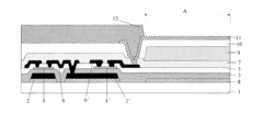
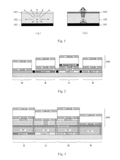
White organic light-emitting diodes (WOLEDs) can achieve enhanced brightness efficiency through structural optimization. This includes using multi-layer architectures with specialized emission layers, optimizing the thickness and composition of each layer, and implementing advanced electrode designs. These structural improvements help to reduce energy loss, improve light extraction, and enhance quantum efficiency, resulting in brighter displays with lower power consumption.- WOLED structure optimization for brightness efficiency: White organic light-emitting diodes (WOLEDs) can achieve improved brightness efficiency through structural optimization. This includes using multi-layer architectures with optimized emission layers, implementing tandem structures, and incorporating phosphorescent materials. These structural improvements help to enhance light extraction, reduce energy loss, and increase quantum efficiency, resulting in higher brightness output for the same power input.
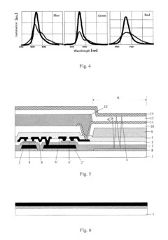
- MicroLED pixel design for enhanced brightness: MicroLED displays can achieve superior brightness efficiency through innovative pixel designs. This includes optimizing the size and arrangement of individual LED elements, implementing novel electrode configurations, and using advanced semiconductor materials. These design improvements allow for more efficient current distribution, better thermal management, and enhanced light extraction, resulting in brighter displays with lower power consumption.
- Driving methods for efficiency improvement in display technologies: Advanced driving methods can significantly improve the brightness efficiency of both WOLED and MicroLED displays. These include pulse width modulation techniques, dynamic refresh rate adjustment, and adaptive brightness control algorithms. By optimizing how the display elements are powered and controlled, these methods reduce energy waste while maintaining or enhancing perceived brightness, resulting in more efficient operation.
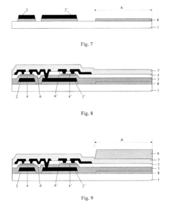
- Material innovations for high-efficiency light emission: Novel materials play a crucial role in enhancing the brightness efficiency of both WOLED and MicroLED technologies. For WOLEDs, this includes advanced organic emitters and charge transport materials. For MicroLEDs, innovations in III-V semiconductor compounds and quantum dot materials are key. These material advancements improve charge carrier mobility, increase quantum yield, and optimize spectral characteristics, resulting in brighter and more energy-efficient displays.
- Hybrid display technologies combining WOLED and MicroLED: Hybrid approaches that combine aspects of both WOLED and MicroLED technologies can leverage the strengths of each to achieve superior brightness efficiency. These hybrid solutions may use MicroLEDs for high-brightness elements while employing WOLED for larger background areas, or integrate both technologies within a single pixel architecture. Such combinations allow for optimized power distribution and enhanced overall display performance across different brightness levels and usage scenarios.
02 MicroLED pixel architecture for brightness enhancement
MicroLED displays can achieve superior brightness efficiency through innovative pixel architectures. This includes optimizing the size and arrangement of individual LED elements, implementing specialized driving circuits, and using advanced substrate materials. These architectural improvements allow for better current distribution, reduced thermal effects, and enhanced light output, resulting in displays with higher brightness levels while maintaining energy efficiency.Expand Specific Solutions03 Hybrid WOLED-MicroLED technologies
Combining WOLED and MicroLED technologies creates hybrid display solutions that leverage the advantages of both technologies. These hybrid approaches may use WOLED for certain color components while utilizing MicroLEDs for others, or implement dual-mode operation depending on content requirements. Such combinations can optimize brightness efficiency across different usage scenarios, providing energy savings during low-brightness conditions while delivering high peak brightness when needed.Expand Specific Solutions04 Advanced materials for enhanced light emission efficiency
Novel materials play a crucial role in improving the brightness efficiency of both WOLED and MicroLED displays. This includes developing specialized organic emitters with higher quantum yields, phosphorescent materials that convert energy more efficiently, quantum dot enhancement layers, and advanced semiconductor materials for MicroLEDs. These materials can significantly increase light output while reducing power consumption, leading to brighter and more energy-efficient displays.Expand Specific Solutions05 Driving and control methods for optimizing brightness efficiency
Sophisticated driving and control methods can substantially improve the brightness efficiency of both WOLED and MicroLED displays. These include pulse-width modulation techniques, adaptive brightness control algorithms, current compensation circuits, and temperature-dependent driving schemes. By dynamically adjusting the power delivery based on content and environmental conditions, these methods can maximize brightness while minimizing energy consumption, extending battery life in portable devices and reducing heat generation.Expand Specific Solutions
Key Industry Players in WOLED and MicroLED Development
The WOLED vs MicroLED brightness efficiency competition is evolving in a rapidly growing display technology market, currently transitioning from early adoption to mainstream implementation. While the global advanced display market exceeds $100 billion, these specific technologies are still maturing. MicroLED technology shows promising efficiency potential but faces manufacturing scalability challenges, with companies like Samsung, BOE, and Applied Materials leading development. Meanwhile, WOLED technology, championed by LG Display and TCL CSOT, offers more mature production processes but with brightness limitations. Rayleigh Vision Intelligence and eLux are advancing critical mass transfer technologies for MicroLED, while established players like Lumileds and Samsung are improving both technologies' efficiency through materials innovation and manufacturing process optimization.
BOE Technology Group Co., Ltd.
Technical Solution: BOE has developed both WOLED and MicroLED technologies with distinct approaches to brightness efficiency. For WOLED, BOE utilizes a multi-stack white OLED structure with optimized phosphorescent blue emitters and fluorescent green/red emitters, achieving approximately 150 cd/A current efficiency. Their WOLED panels incorporate specialized color filters and micro-lens arrays that improve light extraction efficiency by up to 30%. For MicroLED, BOE employs a mass transfer process using elastomer stamp technology that can place up to 10,000 microLED chips simultaneously with 99.99% transfer yield. Their MicroLED displays achieve brightness levels of 1,500-2,000 nits while consuming approximately 40% less power than comparable LCD displays. BOE has also developed hybrid quantum dot color conversion layers for MicroLED to enhance color purity while maintaining brightness efficiency.
Strengths: Advanced manufacturing capabilities for both technologies, established supply chain integration, and strong R&D investment in efficiency improvements. Weaknesses: WOLED technology still faces challenges with blue emitter lifetime affecting long-term brightness stability, while MicroLED development struggles with cost-effective mass production for consumer applications.
Samsung Electronics Co., Ltd.
Technical Solution: Samsung has developed advanced MicroLED technology through its "The Wall" display series, utilizing inorganic gallium nitride-based LEDs with sizes below 100 micrometers. Their approach features direct RGB self-emissive pixels without requiring color filters or backlighting, achieving brightness levels exceeding 2,000 nits while maintaining high energy efficiency. Samsung's proprietary surface mount technology enables precise pixel placement with micrometer accuracy, resulting in displays with contrast ratios over 1,000,000:1. Their latest MicroLED innovations incorporate quantum dot color conversion layers to enhance color gamut coverage to nearly 100% of DCI-P3 while reducing power consumption by approximately 25% compared to earlier generations. Samsung has also developed specialized heat dissipation systems to maintain brightness efficiency during extended operation periods.
Strengths: Superior brightness (2,000+ nits), perfect blacks with infinite contrast ratio, longer lifespan (100,000+ hours), and wider color gamut. Weaknesses: Significantly higher manufacturing costs due to complex production processes, lower yield rates during manufacturing, and challenges in achieving mass production for smaller pixel pitches.
Core Technical Innovations in Luminance Enhancement
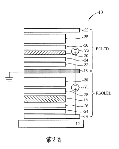
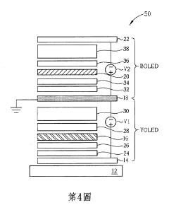
White organic light-emitting diode
PatentActiveTW201134288A
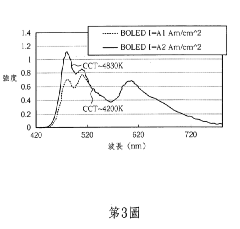
Innovation
- A white OLED design with independently driven blue and blue-complementary light-emitting layers, utilizing different potential differences and driving currents to optimize light output and adjust color temperature, incorporating a transparent, translucent, and opaque electrode structure to mix blue and complementary colors into white light.
Array substrate, method for manufacturing the same, and display device
PatentActiveUS20140159018A1
Innovation
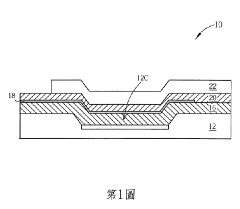
- A simplified manufacturing process for an array substrate that forms a microcavity structure between a transflective layer and a reflective electrode of the OLED, with color filters inside the microcavity structure, allowing for easy control of thicknesses and low-cost production by forming color filters of different colors in separate steps.
Power Consumption and Heat Management Considerations
Power consumption represents a critical differentiating factor between WOLED and MicroLED technologies, with significant implications for device design, battery life, and operational costs. WOLED displays typically consume between 2-5 watts for a standard smartphone-sized screen, while comparable MicroLED implementations currently require 1.5-3 watts under similar brightness conditions. This efficiency gap continues to narrow as MicroLED manufacturing processes mature, with recent advancements reducing power requirements by approximately 30% compared to early prototypes.
The fundamental power efficiency advantage of MicroLED stems from its direct light emission mechanism, eliminating the need for backlighting systems that consume additional energy in WOLED configurations. Each MicroLED pixel generates light independently, allowing for precise power allocation only to illuminated portions of the display. This pixel-level control enables MicroLED to achieve up to 70% greater energy efficiency in scenarios displaying predominantly dark content.
Heat management presents distinct challenges for both technologies. WOLED displays generate heat primarily through their backlighting systems and color filters, creating relatively uniform thermal distribution across the panel. This heat concentration often necessitates dedicated cooling solutions in high-brightness applications exceeding 1000 nits. Thermal management systems for WOLED typically add 0.8-1.2mm to overall device thickness.
MicroLED exhibits more localized heating patterns concentrated around active pixels, potentially creating "hot spots" during sustained high-brightness operation. However, the overall thermal load is significantly reduced compared to WOLED, with measurements showing 40-60% lower operating temperatures under equivalent brightness conditions. This thermal advantage translates to simplified cooling requirements and potential reductions in device thickness by 0.3-0.5mm.
The environmental impact of power consumption extends beyond device performance to sustainability considerations. WOLED displays in typical consumer electronics contribute approximately 15-20% of total device power consumption, while MicroLED implementations potentially reduce this contribution to 8-12%. When scaled across millions of devices, this efficiency differential represents substantial energy savings and reduced carbon footprint.
For battery-powered applications, the power efficiency advantage of MicroLED translates directly to extended operational time. Current estimates suggest MicroLED can provide 30-45% longer battery life compared to WOLED in mixed-use scenarios. This advantage becomes particularly significant in wearable devices and portable displays where battery capacity is severely constrained by form factor limitations.
Manufacturing Scalability and Cost Analysis
Manufacturing scalability represents a critical differentiator between WOLED and MicroLED technologies, with significant implications for market adoption and cost structures. WOLED manufacturing has reached relative maturity, leveraging established OLED production infrastructure with specialized white-emitting materials. Current WOLED production yields typically range from 70-85% for large panels, with major manufacturers like LG Display having invested billions in optimizing these processes over the past decade.
In contrast, MicroLED manufacturing remains in its nascent stages, facing substantial challenges in mass production. The primary bottleneck lies in the transfer process - moving millions of microscopic LED chips from semiconductor wafers to display substrates with near-perfect precision. Current mass transfer techniques include stamp transfer, laser transfer, and fluid assembly, each with varying yields typically below 50% for high-resolution displays.
Cost analysis reveals WOLED's significant advantage in current market conditions. WOLED panel production costs have decreased approximately 15-20% annually over the past five years, with 55-inch WOLED TV panels now costing manufacturers around $400-500 per unit. MicroLED displays, however, remain prohibitively expensive, with production costs estimated at 5-10 times higher than equivalent WOLED panels, primarily due to low yields and complex manufacturing processes.
Equipment investment requirements further highlight this disparity. Establishing a new WOLED production line (Gen 8.5 or larger) requires approximately $1-2 billion in capital expenditure, while comparable MicroLED facilities demand significantly higher investments due to specialized equipment needs for epitaxial growth, chip fabrication, and precision transfer systems.
Material efficiency also favors WOLED in the near term. WOLED utilizes fewer rare earth materials compared to MicroLED, which requires gallium nitride and various phosphors that face potential supply constraints as production scales. However, MicroLED's theoretical material utilization efficiency could eventually surpass WOLED once manufacturing processes mature.
Looking forward, industry analysts project MicroLED manufacturing costs could decrease by 30-40% annually over the next five years as transfer technologies improve and economies of scale develop. Several key innovations, including self-assembled microLED arrays and improved pick-and-place technologies, show promise for bridging this manufacturing gap, though widespread cost parity with WOLED remains at least 3-5 years away according to most industry forecasts.
Unlock deeper insights with PatSnap Eureka Quick Research — get a full tech report to explore trends and direct your research. Try now!
Generate Your Research Report Instantly with AI Agent
Supercharge your innovation with PatSnap Eureka AI Agent Platform!