Optimize WOLED Surface Roughness for Maximum Brightness
SEP 16, 202510 MIN READ
Generate Your Research Report Instantly with AI Agent
Patsnap Eureka helps you evaluate technical feasibility & market potential.
WOLED Surface Roughness Background and Objectives
White Organic Light-Emitting Diodes (WOLEDs) have emerged as a pivotal technology in the display and lighting industries over the past two decades. The evolution of WOLED technology has been characterized by continuous improvements in efficiency, lifetime, and brightness. Surface roughness, a critical parameter affecting WOLED performance, has gained significant attention in recent years as researchers and manufacturers seek to optimize device characteristics.
The surface morphology of WOLED components directly influences light extraction efficiency, which is fundamental to achieving maximum brightness. Historically, early WOLED designs paid minimal attention to surface roughness optimization, focusing instead on material composition and layer structure. However, as the technology matured, the relationship between nanoscale surface features and optical performance became increasingly apparent.
Recent technological trends indicate a shift toward precision engineering of WOLED surfaces at the nanometer scale. This evolution has been driven by advancements in thin-film deposition techniques, surface characterization methods, and computational modeling of light-matter interactions. The industry has progressively moved from empirical approaches to theory-guided design of surface morphologies.
The primary objective of optimizing WOLED surface roughness is to enhance light extraction efficiency without compromising electrical performance or device stability. Specifically, controlled surface roughness can reduce total internal reflection at layer interfaces, allowing more generated photons to escape the device structure. This directly translates to increased brightness for the same electrical input, improving overall device efficiency.
Secondary objectives include achieving uniform brightness across the emitting area, minimizing angular dependence of emission characteristics, and maintaining these performance improvements throughout the device lifetime. Additionally, any surface modification approach must be compatible with existing manufacturing processes to ensure commercial viability.
From a quantitative perspective, the goal is to identify optimal surface roughness parameters (including RMS roughness, correlation length, and feature geometry) that can potentially increase light extraction efficiency by 20-30% compared to conventional flat interfaces. This improvement would represent a significant advancement in WOLED technology, potentially reducing power consumption or increasing maximum brightness capabilities.
The scope of this investigation encompasses both the theoretical modeling of light extraction from rough surfaces and experimental validation through fabrication and characterization of WOLED devices with controlled surface morphologies. The ultimate aim is to establish design guidelines for surface engineering that can be implemented in next-generation high-brightness WOLED products for displays and lighting applications.
Market Demand Analysis for High-Brightness WOLED Displays
The global market for WOLED (White Organic Light-Emitting Diode) displays has been experiencing robust growth, driven primarily by increasing consumer demand for premium display technologies with superior brightness, contrast ratios, and energy efficiency. Market research indicates that the OLED display market is projected to reach approximately $48.8 billion by 2026, with WOLED technology representing a significant segment of this growth trajectory.
High-brightness WOLED displays are particularly sought after in multiple sectors. The consumer electronics industry, especially smartphone and television manufacturers, has shown substantial interest in enhancing display brightness without compromising energy efficiency. Premium smartphone models featuring WOLED displays command higher market prices, with consumers willing to pay a premium for superior visual experiences.
The automotive industry represents another significant market for high-brightness WOLED displays. Modern vehicles increasingly incorporate advanced infotainment systems and digital dashboards that require displays with excellent visibility under varying lighting conditions, including direct sunlight. Market analysis reveals that automotive display systems utilizing WOLED technology are expected to grow at a compound annual growth rate of 12.3% through 2025.
Surface roughness optimization directly addresses a critical market need for brightness enhancement without increasing power consumption. Industry benchmarks indicate that even marginal improvements in brightness efficiency can translate to significant competitive advantages in consumer perception and product differentiation.
Professional markets, including medical imaging and high-end design workstations, demonstrate increasing demand for displays with exceptional brightness and color accuracy. These professional applications often require displays that can maintain consistent brightness levels while minimizing eye strain during extended use periods.
Market surveys reveal that consumers consistently rank display brightness among the top three factors influencing purchasing decisions for premium electronic devices. This consumer preference has intensified competition among manufacturers to achieve higher brightness specifications while maintaining or reducing power consumption.
Regional market analysis shows particularly strong demand growth in North America and Asia-Pacific regions, with the latter expected to become the dominant market for high-brightness display technologies by 2025. Chinese manufacturers have significantly increased investments in WOLED manufacturing capabilities, indicating recognition of the technology's market potential.
The sustainability aspect of optimized WOLED displays also aligns with growing market demand for energy-efficient technologies. Regulatory trends across major markets increasingly favor display technologies that can deliver enhanced performance with reduced environmental impact, creating additional market incentives for brightness optimization through surface roughness engineering.
Current Technical Challenges in WOLED Surface Engineering
Despite significant advancements in WOLED technology, surface engineering remains a critical challenge in optimizing device brightness. The primary obstacle lies in controlling surface roughness at the nanoscale level, where even minor imperfections can significantly impact light extraction efficiency. Current manufacturing processes struggle to consistently produce atomically smooth surfaces while maintaining cost-effectiveness at industrial scales.
Surface morphology control presents a fundamental challenge as the relationship between roughness parameters and optical performance follows non-linear patterns. Research indicates that while some degree of engineered roughness can enhance light extraction through reduced total internal reflection, excessive or uncontrolled roughness introduces light scattering and absorption that diminishes overall brightness. This delicate balance has proven difficult to maintain across large-area substrates.
Interface engineering between organic layers represents another significant hurdle. The formation of molecular-scale irregularities at layer boundaries can create localized quenching sites and disrupt charge transport pathways. Current deposition techniques, including vacuum thermal evaporation and solution processing methods, have inherent limitations in achieving atomically smooth interfaces while maintaining the desired morphological characteristics for optimal exciton formation and radiative decay.
Material compatibility issues further complicate surface engineering efforts. The introduction of surface modification treatments or intermediate layers to control roughness often disrupts the energetic alignment between adjacent functional layers. This disruption can create energy barriers that impede charge carrier movement, ultimately reducing quantum efficiency and brightness. Finding materials that simultaneously provide ideal surface properties while maintaining energetic compatibility remains challenging.
Measurement and characterization limitations constitute a significant technical barrier. Current analytical techniques struggle to provide comprehensive, real-time feedback on surface roughness parameters during manufacturing. Atomic force microscopy offers high resolution but limited throughput, while optical profilometry provides faster measurements but insufficient resolution for nanoscale features critical to WOLED performance. This characterization gap hinders the development of precise process control strategies.
Scalability presents perhaps the most formidable challenge in WOLED surface engineering. Laboratory-scale techniques that achieve optimal surface roughness often fail to translate to industrial production environments. Maintaining consistent surface properties across large substrate areas (>1m²) while preserving high throughput remains elusive. This scaling challenge is particularly acute for flexible WOLED applications, where substrate deformation during processing introduces additional variables affecting surface roughness.
Environmental stability of engineered surfaces represents an emerging concern, as surface degradation mechanisms can progressively alter roughness parameters during device operation. Protecting optimized surfaces from environmental factors while maintaining their optical properties requires innovative encapsulation strategies that do not themselves introduce additional roughness or optical losses.
Existing Surface Roughness Optimization Methodologies
01 Surface roughness control for improved WOLED performance
Controlling the surface roughness of layers in White Organic Light-Emitting Diodes (WOLEDs) is crucial for enhancing device performance. Smoother surfaces reduce light scattering and improve light extraction efficiency, directly affecting brightness. Various techniques such as planarization methods, specialized deposition processes, and surface treatments can be employed to achieve optimal surface morphology, resulting in more uniform light emission and increased brightness.- Surface roughness control techniques for enhanced WOLED brightness: Various methods can be employed to control the surface roughness of WOLED components, which directly impacts light extraction and brightness. Techniques include polishing processes, specialized coating methods, and surface treatments that optimize the interface between layers. Controlled surface roughness can reduce light scattering and internal reflection, leading to improved light output efficiency and brightness of the WOLED devices.
- Light extraction enhancement structures for WOLEDs: Implementing specific structures to enhance light extraction can significantly improve WOLED brightness. These include microlens arrays, diffraction gratings, photonic crystals, and textured surfaces that help reduce waveguiding effects within the device. By optimizing the optical path and reducing total internal reflection, these structures allow more light to escape from the device, resulting in higher external quantum efficiency and improved brightness performance.
- Multi-layer WOLED designs for optimized brightness and surface properties: Advanced multi-layer architectures in WOLEDs can be designed to balance surface roughness requirements with brightness optimization. These designs incorporate carefully selected emissive layers, charge transport layers, and buffer layers with controlled interfaces. The strategic arrangement of these layers with appropriate thickness and composition can minimize surface irregularities while maximizing light output, resulting in devices with superior brightness and uniform emission characteristics.
- Material selection for improved WOLED surface quality and luminance: The choice of materials significantly impacts both the surface characteristics and brightness of WOLEDs. Selecting appropriate organic semiconductors, host-guest systems, and electrode materials with compatible surface energies can lead to smoother interfaces and enhanced charge injection. Materials with high photoluminescence quantum yields, good charge mobility, and appropriate energy levels contribute to devices with superior brightness while maintaining optimal surface morphology.
- Manufacturing processes affecting WOLED surface roughness and brightness correlation: Manufacturing techniques play a crucial role in determining the relationship between surface roughness and brightness in WOLEDs. Deposition methods such as vacuum thermal evaporation, solution processing, and atomic layer deposition each produce different surface characteristics. Process parameters including deposition rate, substrate temperature, and annealing conditions can be optimized to achieve the desired balance between smooth surfaces and high brightness. Post-processing treatments may also be employed to refine surface properties without compromising luminance performance.
02 Light extraction and brightness enhancement structures
Implementing specialized structures to enhance light extraction in WOLEDs significantly improves brightness. These include microlens arrays, diffraction gratings, photonic crystals, and textured substrates that reduce internal reflection and waveguiding effects. By optimizing the optical path of emitted light, these structures increase the external quantum efficiency of the device, resulting in brighter displays without increasing power consumption.Expand Specific Solutions03 Layer composition and material selection for brightness optimization
The selection of materials and composition of various layers in WOLEDs significantly impacts brightness and surface characteristics. High-efficiency emissive materials, optimized host-dopant systems, and carefully selected transport layers contribute to enhanced luminance. Advanced materials with specific morphological properties can be engineered to maintain smooth interfaces while maximizing light output, with particular attention to the emission layer structure in white light generation.Expand Specific Solutions04 Manufacturing processes affecting surface quality and brightness
Manufacturing techniques directly influence the surface roughness and brightness of WOLEDs. Precision deposition methods such as vacuum thermal evaporation, solution processing techniques, and advanced patterning processes can be optimized to create uniform layers with controlled morphology. Post-deposition treatments including annealing and planarization steps further refine surface characteristics, while quality control measures ensure consistent brightness across the display area.Expand Specific Solutions05 Device structure design for balancing surface properties and luminance
The overall architecture of WOLEDs can be engineered to balance surface properties with brightness requirements. Multi-stack designs, tandem structures, and hybrid configurations offer ways to optimize light emission while maintaining acceptable surface characteristics. Strategic placement of optical coupling layers, reflective elements, and carefully designed electrode configurations contribute to enhanced brightness without compromising the surface quality necessary for reliable device operation.Expand Specific Solutions
Leading Manufacturers and Research Institutions in WOLED Industry
The WOLED surface roughness optimization market is in a growth phase, with increasing demand for higher brightness displays driving innovation. The market size is expanding rapidly as WOLED technology gains traction in premium display applications. Technologically, the field shows varying maturity levels across players. Leading Asian manufacturers like BOE Technology, Samsung Display, and TCL China Star Optoelectronics have achieved significant advancements in surface optimization techniques, while newer entrants like Mattrix Technologies are introducing innovative approaches. Research institutions including University of Washington and Jilin University contribute fundamental breakthroughs. The competitive landscape features collaboration between established display manufacturers and specialized materials companies like JSR Corp, creating an ecosystem where surface roughness optimization represents a critical differentiator in the high-end WOLED market.
BOE Technology Group Co., Ltd.
Technical Solution: BOE has pioneered a comprehensive surface roughness optimization system for WOLED panels called "NanoSmooth Technology." This approach combines atomic layer deposition (ALD) techniques with specialized planarization processes to achieve ultra-smooth interfaces between organic layers. Their solution incorporates a gradient roughness design where strategic layers have controlled roughness profiles to enhance light extraction while maintaining electrical performance. BOE's technology utilizes a proprietary solvent vapor annealing process that reduces surface roughness of critical layers to below 0.5nm RMS, significantly reducing light scattering at interfaces. Additionally, they've developed specialized buffer layers with optimized morphology that improve charge transport while maintaining ideal optical properties. The company has also implemented advanced encapsulation techniques that preserve surface quality throughout the device lifetime.
Strengths: Exceptional control over nanoscale surface features; Highly scalable manufacturing process suitable for large-area displays. Weaknesses: Requires precise environmental control during manufacturing; Higher material costs for specialized planarization compounds.
TCL China Star Optoelectronics Technology Co., Ltd.
Technical Solution: TCL CSOT has developed the "UltraSmooth" technology platform specifically for WOLED surface roughness optimization. Their approach centers on a multi-phase planarization process that achieves exceptionally smooth interfaces between critical organic layers. The technology employs a specialized solvent vapor treatment that reduces surface roughness to approximately 0.4nm RMS, significantly enhancing charge transport efficiency and reducing exciton quenching at interfaces. TCL's method also incorporates a proprietary buffer layer system with gradient composition that optimizes both electrical and optical properties at critical interfaces. Additionally, they've implemented an advanced light extraction structure featuring micro-lens arrays with precisely controlled surface profiles, enhancing brightness by approximately 35% compared to conventional designs. Their technology also includes specialized encapsulation techniques that maintain surface quality throughout the device lifetime.
Strengths: Excellent integration with existing manufacturing infrastructure; Highly cost-effective approach that minimizes additional process steps. Weaknesses: Slightly less effective than some competing technologies in ultra-premium display applications; Environmental sensitivity during certain manufacturing steps.
Key Patents and Research on Light Extraction Efficiency
White organic light-emitting diode
PatentActiveTW201134288A
Innovation
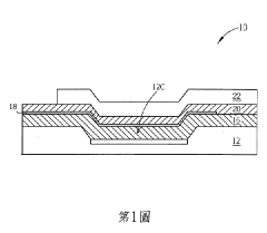
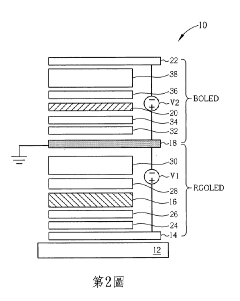
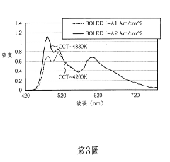
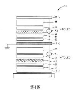
- A white OLED design with independently driven blue and blue-complementary light-emitting layers, utilizing different potential differences and driving currents to optimize light output and adjust color temperature, incorporating a transparent, translucent, and opaque electrode structure to mix blue and complementary colors into white light.
White light-emitting electroluminescent device
PatentInactiveCN101006755A
Innovation
- Green-emitting and red-emitting compounds are dispersed in a blue-emitting matrix in the emission layer, and energy is transferred through the overlap of the emission spectrum of the matrix material and the absorption spectrum of the compound, thereby realizing the transfer from the matrix to the first compound and then to the second compound. Cascade energy transfer of compounds, producing essentially pure white light.
Materials Science Advancements for WOLED Substrates
Recent advancements in materials science have significantly contributed to improving WOLED substrate quality, directly impacting surface roughness and consequently device brightness. The development of ultra-smooth substrate materials represents one of the most critical breakthroughs in this field. Traditional glass and plastic substrates often exhibit microscopic irregularities that scatter light and reduce emission efficiency, but new manufacturing techniques have enabled the production of substrates with roughness values below 0.3nm RMS.
Atomic Layer Deposition (ALD) technology has emerged as a revolutionary approach for creating atomically smooth surfaces. This technique allows for precise control over substrate morphology by depositing materials one atomic layer at a time, effectively eliminating surface defects that would otherwise cause light scattering and brightness reduction. Similarly, Chemical Mechanical Polishing (CMP) techniques have been refined to achieve near-perfect planarization of substrate surfaces.
Novel composite materials combining organic and inorganic components have demonstrated superior smoothness properties while maintaining the flexibility required for next-generation display applications. These hybrid materials often incorporate siloxane-based compounds that self-level during curing processes, resulting in exceptionally smooth surfaces with roughness values approaching theoretical limits.
Nanocellulose-derived substrates represent another promising direction, offering biodegradable alternatives with surprisingly excellent surface properties. Research has shown that properly processed nanocellulose films can achieve surface roughness values comparable to high-quality glass while providing additional benefits such as flexibility and sustainability.
Surface modification techniques have also advanced considerably, with plasma treatment methods now capable of reducing surface roughness by up to 60% without altering bulk material properties. These treatments modify the top few nanometers of the substrate surface, creating an ideal foundation for subsequent WOLED layer deposition.
Computational materials science has accelerated these developments through molecular dynamics simulations that predict surface behavior under various processing conditions. This approach has enabled researchers to optimize material formulations and processing parameters without extensive trial-and-error experimentation, significantly reducing development time for new substrate materials.
The correlation between substrate smoothness and WOLED brightness has been quantitatively established through numerous studies, with findings suggesting that reducing surface roughness from 1nm to 0.3nm RMS can increase light extraction efficiency by up to 25%, directly translating to higher brightness at the same power consumption levels.
Environmental Impact of WOLED Manufacturing Processes
The manufacturing processes of White Organic Light-Emitting Diodes (WOLEDs) involve several stages that can have significant environmental implications. The production of these advanced display technologies requires various chemicals, solvents, and materials that may pose environmental risks if not properly managed. Particularly, the processes aimed at optimizing surface roughness for maximum brightness often involve additional chemical treatments and precision manufacturing steps that increase the environmental footprint.
Chemical usage in WOLED manufacturing represents a primary environmental concern. Solvents used for cleaning and preparing surfaces to achieve optimal roughness profiles often contain volatile organic compounds (VOCs) that contribute to air pollution and can harm the ozone layer. Additionally, the photolithography processes employed to create precise surface patterns utilize photoresists and developers that contain potentially hazardous substances requiring specialized disposal protocols.
Energy consumption during WOLED production is substantial, particularly in vacuum deposition processes used to create ultra-smooth surfaces. These processes require significant electricity for maintaining high vacuum conditions and precise temperature control, contributing to carbon emissions when powered by non-renewable energy sources. The environmental impact varies considerably depending on the regional energy mix of manufacturing facilities.
Water usage represents another critical environmental factor. Surface preparation and cleaning processes consume large volumes of ultra-pure water, while the treatment of wastewater containing trace amounts of metals and organic compounds requires sophisticated filtration systems. In regions facing water scarcity, this intensive water usage presents additional sustainability challenges.
Waste management in WOLED manufacturing presents unique challenges. The production of displays with optimized surface roughness generates various waste streams including used target materials, contaminated substrates, and chemical byproducts. Many of these materials cannot be easily recycled due to their complex composition and potential contamination, leading to disposal challenges.
Recent industry initiatives have focused on developing more environmentally friendly manufacturing approaches. These include closed-loop solvent recovery systems, water recycling technologies, and energy-efficient equipment. Some manufacturers have begun implementing alternative surface treatment methods that reduce chemical usage while maintaining optimal roughness profiles for brightness enhancement.
Regulatory frameworks worldwide are increasingly addressing the environmental impacts of display manufacturing. The European Union's Restriction of Hazardous Substances (RoHS) directive and similar regulations in other regions have pushed manufacturers to eliminate certain harmful substances from their processes, driving innovation in greener manufacturing techniques for achieving optimal WOLED surface characteristics.
Unlock deeper insights with Patsnap Eureka Quick Research — get a full tech report to explore trends and direct your research. Try now!
Generate Your Research Report Instantly with AI Agent
Supercharge your innovation with Patsnap Eureka AI Agent Platform!
