Enhance WOLED Color Purity With Refined Material Systems
SEP 16, 20259 MIN READ
Generate Your Research Report Instantly with AI Agent
Patsnap Eureka helps you evaluate technical feasibility & market potential.
WOLED Technology Evolution and Objectives
White Organic Light-Emitting Diode (WOLED) technology has evolved significantly since its inception in the late 1980s. The journey began with single-layer devices exhibiting low efficiency and poor stability, progressing through various architectural innovations to today's sophisticated multi-layer structures. This evolution has been driven by the persistent pursuit of higher efficiency, better color reproduction, and extended operational lifetimes.
The fundamental challenge in WOLED technology has always been achieving pure white light emission while maintaining high efficiency and stability. Early WOLEDs utilized a combination of red, green, and blue emitting materials in a single layer, resulting in spectral overlap and color contamination. The introduction of multi-layer structures in the early 2000s marked a significant advancement, allowing for better control of charge transport and recombination zones.
A critical milestone was reached with the development of phosphorescent materials, particularly iridium-based complexes, which enabled internal quantum efficiencies approaching 100%. However, these materials presented challenges in achieving stable blue emission, leading to color shifts over device lifetime. The subsequent introduction of thermally activated delayed fluorescence (TADF) materials around 2012 offered a potential solution, providing high efficiency without relying on precious metals.
Recent years have witnessed the emergence of hybrid WOLED architectures combining fluorescent blue emitters with phosphorescent green and red emitters, balancing efficiency and stability. Concurrently, quantum dot-enhanced WOLEDs have demonstrated promising results in achieving narrower emission spectra and thus improved color purity.
The primary objective in enhancing WOLED color purity through refined material systems is to develop emitter materials with narrower emission spectra while maintaining high quantum efficiency. This involves molecular engineering to reduce vibronic coupling and minimize spectral overlap between different color emitters. Additionally, there is a focus on developing host materials with wider bandgaps and appropriate energy levels to confine charge carriers effectively within the emissive layer.
Another crucial objective is improving the stability of blue emitters, which remain the weakest link in WOLED technology. This includes exploring new molecular designs that distribute electronic stress more effectively and incorporating stabilizing moieties to prevent degradation pathways. Furthermore, there is significant interest in developing solution-processable materials to enable cost-effective manufacturing techniques such as inkjet printing, potentially revolutionizing WOLED production.
The ultimate goal is to create WOLED systems that not only meet but exceed the color reproduction capabilities of traditional display technologies while maintaining the inherent advantages of OLEDs, such as flexibility, transparency, and energy efficiency.
Market Analysis for High Color Purity WOLED Applications
The WOLED (White Organic Light-Emitting Diode) market is experiencing significant growth, driven by increasing demand for high-quality display technologies across multiple sectors. The global OLED market, valued at approximately $38.4 billion in 2021, is projected to reach $72.8 billion by 2026, with WOLEDs representing a substantial segment of this expansion. The compound annual growth rate (CAGR) for the WOLED market specifically is estimated at 14.7% through 2027, outpacing many other display technologies.
High color purity WOLEDs are particularly sought after in premium consumer electronics, where manufacturers compete intensely on display quality metrics. The smartphone segment currently dominates WOLED application, accounting for 46% of market share, followed by televisions (27%), wearable devices (12%), and automotive displays (8%). Industry analysts predict that automotive applications will see the fastest growth rate at 22.3% CAGR through 2028, as luxury vehicle manufacturers increasingly adopt WOLED technology for instrument clusters and infotainment systems.
Consumer demand for enhanced visual experiences is driving the need for WOLEDs with superior color gamut coverage. Market research indicates that devices offering over 95% DCI-P3 color gamut coverage command a 15-22% price premium compared to those with standard color performance. This price differential has created a strong economic incentive for manufacturers to invest in high color purity WOLED technologies.
Regional analysis shows Asia-Pacific dominating WOLED manufacturing with 78% of global production capacity, led by South Korea, Japan, and China. However, North America and Europe represent the largest markets for high-end applications requiring superior color purity, with combined consumption of 52% of premium WOLED displays.
The healthcare visualization market represents an emerging high-value application for high color purity WOLEDs, with medical imaging displays requiring exceptional color accuracy for diagnostic purposes. This segment is growing at 18.6% annually and commands the highest margins in the WOLED ecosystem, with devices selling at 3-4 times the price of consumer-grade displays of equivalent size.
Industry surveys indicate that 87% of professional users in creative fields (photography, video editing, graphic design) consider color accuracy a critical purchasing factor, creating a stable niche market for high-performance WOLEDs. Additionally, the gaming market has emerged as a significant driver, with 64% of premium gaming monitors now featuring OLED technology, up from just 12% in 2019.
Current WOLED Material Systems and Limitations
White Organic Light-Emitting Diodes (WOLEDs) have emerged as a promising technology for display and lighting applications due to their energy efficiency, flexibility, and potential for low-cost manufacturing. Current WOLED material systems primarily utilize three approaches: multi-component emissive layers, tandem structures, and down-conversion techniques. Each system presents distinct advantages but also faces significant limitations in achieving optimal color purity.
Multi-component emissive layer systems typically combine blue, green, and red emitters within a single layer or in adjacent layers. While this approach offers manufacturing simplicity, it suffers from energy transfer complications between different chromophores, leading to color contamination. The proximity of different emitters often results in Förster Resonance Energy Transfer (FRET), which can diminish color purity and reduce device efficiency. Additionally, differential aging rates among various emitters cause color shift over the device lifetime.
Tandem WOLED structures stack multiple OLED units vertically, connected by charge generation layers. This architecture allows for independent optimization of each emissive unit but introduces complexity in manufacturing and increases material costs. The optical coupling between stacked units can create interference effects that alter the emission spectrum, compromising color purity. Furthermore, the increased number of interfaces in tandem structures can lead to charge accumulation and subsequent degradation of device performance.
Down-conversion systems employ blue OLEDs combined with color-converting materials such as quantum dots or phosphors. While this approach simplifies the emitter design, it faces challenges in conversion efficiency and stability. The down-conversion materials often exhibit photodegradation under continuous excitation, leading to diminished color quality over time. Additionally, incomplete conversion of blue light results in spectral contamination, reducing the color gamut achievable by these systems.
A critical limitation across all current WOLED material systems is the trade-off between color purity and efficiency. High color purity typically requires narrow emission bands, which inherently limit the photon output. Conversely, broader emission spectra yield higher efficiency but compromise color saturation. This fundamental challenge is exacerbated by the molecular design constraints of organic emitters, which often exhibit broad emission profiles due to vibronic coupling and conformational diversity.
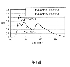
Material stability presents another significant limitation, particularly for blue emitters which operate at higher energy levels and are more susceptible to degradation. The differential aging of emissive materials leads to color point drift over the device lifetime, compromising long-term color stability. This issue is particularly pronounced in displays where color accuracy is paramount.
Multi-component emissive layer systems typically combine blue, green, and red emitters within a single layer or in adjacent layers. While this approach offers manufacturing simplicity, it suffers from energy transfer complications between different chromophores, leading to color contamination. The proximity of different emitters often results in Förster Resonance Energy Transfer (FRET), which can diminish color purity and reduce device efficiency. Additionally, differential aging rates among various emitters cause color shift over the device lifetime.
Tandem WOLED structures stack multiple OLED units vertically, connected by charge generation layers. This architecture allows for independent optimization of each emissive unit but introduces complexity in manufacturing and increases material costs. The optical coupling between stacked units can create interference effects that alter the emission spectrum, compromising color purity. Furthermore, the increased number of interfaces in tandem structures can lead to charge accumulation and subsequent degradation of device performance.
Down-conversion systems employ blue OLEDs combined with color-converting materials such as quantum dots or phosphors. While this approach simplifies the emitter design, it faces challenges in conversion efficiency and stability. The down-conversion materials often exhibit photodegradation under continuous excitation, leading to diminished color quality over time. Additionally, incomplete conversion of blue light results in spectral contamination, reducing the color gamut achievable by these systems.
A critical limitation across all current WOLED material systems is the trade-off between color purity and efficiency. High color purity typically requires narrow emission bands, which inherently limit the photon output. Conversely, broader emission spectra yield higher efficiency but compromise color saturation. This fundamental challenge is exacerbated by the molecular design constraints of organic emitters, which often exhibit broad emission profiles due to vibronic coupling and conformational diversity.
Material stability presents another significant limitation, particularly for blue emitters which operate at higher energy levels and are more susceptible to degradation. The differential aging of emissive materials leads to color point drift over the device lifetime, compromising long-term color stability. This issue is particularly pronounced in displays where color accuracy is paramount.
State-of-the-Art Color Purity Enhancement Techniques
01 Multi-layer structure design for improved color purity
WOLED devices can achieve enhanced color purity through carefully designed multi-layer structures. By optimizing the arrangement of emission layers, electron transport layers, and hole transport layers, manufacturers can control the spectral output of the device. These structures often incorporate specific dopants in precise concentrations within each layer to achieve balanced white light emission with high color purity. The thickness and composition of each layer significantly impacts the final color coordinates and purity of the emitted white light.- Multi-layer structure design for color purity enhancement: WOLED devices can achieve improved color purity through strategic multi-layer structures. By carefully designing the arrangement of emission layers, electron transport layers, and hole transport layers, manufacturers can control the light emission spectrum. These structures often incorporate color filters or wavelength conversion materials to refine the white light output, resulting in more precise color rendering and higher purity white emission.
- Dopant and host material selection for spectrum optimization: The selection of appropriate dopant and host materials plays a crucial role in achieving high color purity in WOLEDs. By combining specific phosphorescent or fluorescent dopants with compatible host materials, manufacturers can tune the emission spectrum to achieve balanced white light. The concentration ratios of red, green, and blue emitters are carefully controlled to produce white light with high color purity and stability over the device lifetime.
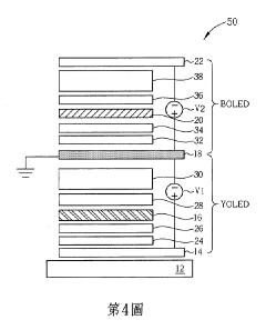
- Tandem WOLED architecture for improved color performance: Tandem WOLED structures, which stack multiple emission units vertically with charge generation layers in between, can significantly enhance color purity. This architecture allows for independent optimization of different color emission units, enabling precise control over the overall white light spectrum. The approach reduces color shift at different brightness levels and viewing angles, resulting in more consistent and pure white light emission.
- Quantum dot integration for narrow-band emission: Incorporating quantum dots into WOLED structures provides narrow emission bandwidths that enhance color purity. These nanoscale semiconductor particles can be tuned to emit specific wavelengths by controlling their size and composition. When integrated with organic materials in hybrid structures, quantum dots help achieve more saturated colors and a wider color gamut, resulting in white light with higher purity and better color rendering properties.
- Color correction filters and optical enhancement techniques: External optical components and color correction techniques can significantly improve the perceived color purity of WOLEDs. These include specialized microlens arrays, color filters, and optical outcoupling structures that modify the emitted light. Advanced color management algorithms and compensation techniques can also be employed to adjust the emission characteristics in real-time, maintaining high color purity despite aging effects or temperature variations.
02 Color filtering technology for WOLED displays
Color filtering techniques are employed to improve the color purity of WOLEDs by selectively transmitting specific wavelengths of light. These filters can be integrated directly into the OLED structure or applied as an additional layer. Advanced color filter designs can enhance color gamut and purity by reducing spectral overlap between different color channels. Some approaches combine color filters with micro-cavity structures to further refine the spectral output and achieve more saturated colors while maintaining the efficiency benefits of white OLED technology.Expand Specific Solutions03 Emissive material selection and composition
The selection and composition of emissive materials play a crucial role in determining WOLED color purity. By carefully choosing organic emitters with complementary emission spectra, manufacturers can create white light with specific color characteristics. Phosphorescent materials, fluorescent materials, or combinations of both can be utilized to achieve the desired spectral output. The ratio and concentration of different emitters (red, green, and blue) significantly impact the resulting white light quality. Novel emissive materials with narrow emission bands help reduce spectral overlap and improve color purity.Expand Specific Solutions04 Tandem WOLED architecture for color balance
Tandem WOLED architectures utilize multiple emission units stacked vertically and connected by charge generation layers. This approach allows for better control over the contribution of each color component to the final white light emission. By independently optimizing each emission unit, manufacturers can achieve improved color purity while maintaining high efficiency. The tandem structure enables precise tuning of the spectral power distribution, resulting in white light with specific color temperature and purity characteristics. This architecture also helps address the differential aging of different color emitters, maintaining color stability over the device lifetime.Expand Specific Solutions05 Micro-cavity and optical optimization techniques
Micro-cavity structures and optical optimization techniques can significantly enhance WOLED color purity. By controlling the optical path length within the device through carefully designed reflective layers and transparent electrodes, the spectral characteristics of emitted light can be tuned. Resonant cavity effects can be leveraged to enhance desired wavelengths while suppressing others. Advanced optical designs incorporate quantum well structures, photonic crystals, or plasmonic elements to manipulate light emission. These techniques allow for narrower emission bands, resulting in improved color purity without sacrificing efficiency.Expand Specific Solutions
Leading WOLED Material and Display Manufacturers
The WOLED color purity enhancement market is currently in a growth phase, with increasing demand for higher quality displays driving innovation in material systems. The global OLED market is projected to reach approximately $48 billion by 2023, with WOLED technology gaining traction due to its efficiency advantages. Technologically, the field shows varying maturity levels across companies. Universal Display Corporation leads with pioneering phosphorescent OLED materials, while Asian manufacturers like LG Display, BOE, and TCL China Star are advancing rapidly in commercialization. Research institutions including Technical Institute of Physics & Chemistry CAS and University of Southern California contribute fundamental breakthroughs. Semiconductor Energy Laboratory and Idemitsu Kosan are developing novel material systems specifically targeting color purity challenges, positioning themselves as key players in this specialized segment.
BOE Technology Group Co., Ltd.
Technical Solution: BOE Technology has developed an advanced approach to enhancing WOLED color purity through refined material systems and innovative device architectures. Their technology employs a tandem WOLED structure with multiple emission units connected by charge generation layers, allowing for independent optimization of different color components[7]. BOE's material system incorporates specially engineered host materials with high triplet energy levels paired with phosphorescent dopants to achieve high efficiency and color purity. Their blue emission layers utilize novel thermally activated delayed fluorescence (TADF) materials that achieve higher efficiency than conventional fluorescent emitters while maintaining good color coordinates. BOE has also implemented advanced optical designs including microcavity effects and specialized color filters to further enhance color purity[8]. Their recent developments include hybrid quantum dot-OLED technologies where quantum dot color conversion layers are combined with WOLED backplanes to achieve wider color gamut while maintaining the efficiency and manufacturing advantages of white OLED technology.
Strengths: Rapidly growing manufacturing capacity and technical capabilities; vertical integration from materials to finished displays; strong government support for technology development. Weaknesses: Less established OLED intellectual property portfolio compared to some competitors; relatively newer entrant to WOLED manufacturing; challenges in achieving consistent high-volume production yields.
Universal Display Corp.
Technical Solution: Universal Display Corporation has pioneered phosphorescent OLED (PHOLED) technology to enhance WOLED color purity. Their approach involves developing novel emitter materials with narrow emission spectra and high color saturation. UDC's proprietary PHOLED technology utilizes phosphorescent emitters that achieve nearly 100% internal quantum efficiency compared to 25% for conventional fluorescent materials[1]. Their refined material systems include advanced host-dopant combinations where carefully selected host materials are doped with precisely engineered phosphorescent emitters to optimize energy transfer and prevent triplet-triplet annihilation. UDC has also developed multi-layer WOLED structures with separate red, green, and blue emission layers, allowing for independent optimization of each color component[2]. Their latest innovations include thermally activated delayed fluorescence (TADF) emitters and hybrid fluorescent-phosphorescent systems to address blue emitter efficiency and lifetime challenges.
Strengths: Industry-leading phosphorescent materials with nearly 100% internal quantum efficiency; extensive patent portfolio covering key OLED materials and architectures; strong partnerships with major display manufacturers. Weaknesses: Challenges with blue phosphorescent emitter stability and lifetime; higher manufacturing costs compared to some competing technologies; dependence on licensing business model.
Critical Patents in WOLED Material Engineering
White organic light-emitting diode
PatentActiveTW201134288A
Innovation
- A white OLED design with independently driven blue and blue-complementary light-emitting layers, utilizing different potential differences and driving currents to optimize light output and adjust color temperature, incorporating a transparent, translucent, and opaque electrode structure to mix blue and complementary colors into white light.
White organic light-emitting diode
PatentActiveUS7723914B2
Innovation
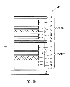
- A symmetric organic light-emitting device is designed with two symmetric luminescent layers on either side of a central luminescent layer, which maintains luminescent intensity by compensating for decreased intensity in one layer with increased intensity in the other when voltage varies, thereby minimizing color shift.
Environmental Impact of Advanced WOLED Materials
The environmental implications of advanced WOLED materials represent a critical dimension in the evolution of display technologies. As manufacturers pursue enhanced color purity through refined material systems, the ecological footprint of these innovations demands thorough examination. Current WOLED production processes involve numerous rare earth elements and heavy metals, including iridium, platinum, and europium, whose extraction generates significant environmental degradation through habitat destruction, water pollution, and energy-intensive mining operations.
Material refinement techniques aimed at improving color purity often introduce additional chemical processes that generate hazardous byproducts. The synthesis of high-purity phosphorescent dopants typically requires halogenated solvents and metal catalysts that pose substantial environmental risks if improperly managed. Furthermore, the ultra-high purity requirements for these materials necessitate multiple purification cycles, each consuming considerable energy and chemical resources.
The manufacturing of advanced WOLED panels incorporates increasingly complex multi-layer structures to achieve superior color performance. This complexity translates to extended production times, higher energy consumption, and greater material wastage during fabrication. Vacuum thermal evaporation processes, essential for precise deposition of organic layers, are particularly energy-intensive and contribute significantly to the carbon footprint of WOLED production.
End-of-life considerations present another environmental challenge. The intricate integration of multiple organic and inorganic materials in modern WOLED displays complicates recycling efforts. Separation of these components often requires chemical treatments that generate additional waste streams. The presence of novel compounds with unknown environmental persistence and toxicity profiles raises concerns about long-term ecological impacts.
Several promising approaches are emerging to address these environmental challenges. Bio-based alternatives to traditional petroleum-derived host materials show potential for reducing carbon footprint while maintaining optical performance. Solvent-free manufacturing techniques and more efficient deposition methods could substantially reduce chemical waste and energy consumption. Additionally, designing material systems with recyclability in mind—such as using reversible bonding chemistry—may facilitate future material recovery and reuse.
Regulatory frameworks worldwide are increasingly focusing on the environmental impact of electronic components, with particular attention to rare materials and toxic substances. Manufacturers pursuing enhanced color purity must navigate these evolving regulations while developing commercially viable solutions, creating both challenges and opportunities for innovation in environmentally responsible WOLED technologies.
Manufacturing Scalability of Refined WOLED Systems
The scalability of manufacturing processes for refined WOLED material systems represents a critical factor in their commercial viability. Current production methods for high-purity WOLED materials face significant challenges when transitioning from laboratory-scale synthesis to mass production. The primary obstacle lies in maintaining consistent molecular structure and purity levels across large production batches, which directly impacts color performance and device efficiency.
Vacuum thermal evaporation (VTE) remains the dominant deposition technique for WOLED manufacturing, offering precise layer control but presenting scalability limitations for refined material systems. The process requires stringent temperature control and vacuum conditions that become increasingly difficult to maintain uniformly across larger substrate areas. Recent advancements in linear source evaporation technology have improved material utilization efficiency from 15% to approximately 60%, significantly reducing production costs for refined WOLED systems.
Solution-processing methods, including spin-coating and inkjet printing, offer promising alternatives for scaling production of certain refined WOLED materials. These techniques demonstrate particular advantages for phosphorescent host materials and certain color-enhancing dopants. However, challenges persist in achieving the layer uniformity and interface quality necessary for high-purity color performance, especially when incorporating novel quantum dot color filters or specialized phosphorescent materials.
Equipment manufacturers have developed specialized deposition systems for refined WOLED materials, featuring advanced in-situ monitoring capabilities that ensure consistent film quality. These systems incorporate real-time optical monitoring and automated correction mechanisms that maintain color purity specifications across production runs. The integration of AI-driven process control has further enhanced manufacturing consistency, with reported color variation reduced by up to 40% compared to conventional systems.
Supply chain considerations also impact manufacturing scalability, as refined material systems often require specialty chemicals with limited production capacity. Strategic partnerships between WOLED manufacturers and material suppliers have emerged to secure consistent access to high-purity precursors. Several major display manufacturers have established dedicated material synthesis facilities to ensure quality control throughout the production pipeline, though this vertical integration approach requires substantial capital investment.
Yield rates for refined WOLED systems have improved significantly, with current industry benchmarks reaching 85-90% for high-end displays. This improvement stems from enhanced material purification techniques and more precise deposition control. However, maintaining these yield rates while scaling to larger substrate sizes (Gen 8.5 and beyond) remains an ongoing challenge that requires continued innovation in both materials and manufacturing equipment.
Unlock deeper insights with Patsnap Eureka Quick Research — get a full tech report to explore trends and direct your research. Try now!
Generate Your Research Report Instantly with AI Agent
Supercharge your innovation with Patsnap Eureka AI Agent Platform!