How to Reduce WOLED Electrode Resistance for High Conductivity
SEP 16, 20259 MIN READ
Generate Your Research Report Instantly with AI Agent
Patsnap Eureka helps you evaluate technical feasibility & market potential.
WOLED Electrode Resistance Background and Objectives
White Organic Light-Emitting Diodes (WOLEDs) have emerged as a revolutionary technology in the display and lighting industries over the past two decades. The evolution of WOLED technology has been marked by continuous improvements in efficiency, lifetime, and color quality. However, electrode resistance remains a critical bottleneck limiting the performance of large-area WOLED devices, particularly as the industry moves toward larger displays and lighting panels.
Historically, WOLED electrodes have primarily relied on transparent conductive oxides (TCOs), with indium tin oxide (ITO) being the dominant material since the early 2000s. While ITO offers reasonable conductivity and transparency, its inherent sheet resistance (typically 10-20 Ω/sq) becomes increasingly problematic as device dimensions scale up, leading to voltage drops across the panel and non-uniform luminance.
The technical objective of reducing WOLED electrode resistance is multifaceted. Primary goals include achieving sheet resistance below 5 Ω/sq while maintaining optical transparency above 85% in the visible spectrum, ensuring compatibility with existing manufacturing processes, and maintaining or improving device lifetime. Additionally, any solution must be cost-effective for mass production and ideally reduce dependence on scarce materials like indium.
Recent technological trends indicate a shift toward composite electrode structures, nanomaterial integration, and alternative TCO formulations. The industry has witnessed growing interest in silver nanowire networks, graphene-based electrodes, and metal mesh structures as potential solutions to the resistance challenge. Each approach presents unique advantages and limitations regarding conductivity, transparency, and manufacturing complexity.
Environmental considerations have also become increasingly important in electrode development, with regulations on hazardous materials and sustainability concerns driving research toward more eco-friendly alternatives. The reduction of rare earth elements and implementation of recyclable materials align with global sustainability initiatives and corporate social responsibility goals.
The achievement of high-conductivity electrodes would enable several technological breakthroughs, including truly flexible large-area displays, transparent WOLED lighting with uniform emission, and reduced power consumption in existing applications. These advancements could potentially open new market segments and application areas previously limited by electrode performance constraints.
As we look toward future developments, the integration of multifunctional electrodes that combine high conductivity with additional properties such as flexibility, stretchability, or self-healing capabilities represents the next frontier in WOLED electrode technology. The convergence of nanotechnology, materials science, and electrical engineering will be crucial in addressing this complex technical challenge.
Market Demand Analysis for High Conductivity WOLED
The WOLED (White Organic Light-Emitting Diode) market has experienced significant growth in recent years, driven by increasing demand for high-quality displays in consumer electronics, automotive interfaces, and lighting applications. Market research indicates that the global OLED display market is projected to reach $48.8 billion by 2026, with WOLED technology representing a substantial segment of this market due to its superior color reproduction and energy efficiency.
The demand for high conductivity WOLED technology is particularly pronounced in large-area display applications, where electrode resistance becomes a critical limiting factor. As display sizes increase in television and professional monitor segments, the need for reduced electrode resistance becomes paramount to maintain uniform brightness and prevent voltage drops across the display surface. Industry data shows that the large-format OLED TV market has been growing at approximately 30% annually, creating urgent demand for improved electrode conductivity solutions.
Commercial sectors including digital signage, retail displays, and architectural lighting represent emerging markets with substantial growth potential for high conductivity WOLED technology. These applications require displays with minimal power consumption while maintaining exceptional visual performance across large surface areas, directly benefiting from advances in electrode conductivity.
The automotive industry presents another significant market opportunity, with premium vehicle manufacturers increasingly adopting OLED technology for dashboard displays, entertainment systems, and innovative lighting solutions. This sector demands highly reliable display technologies capable of operating under variable temperature conditions, where consistent conductivity across electrodes is essential for product longevity and performance.
Healthcare and medical imaging applications are creating specialized demand for high-resolution WOLED displays with uniform brightness and excellent color accuracy. The medical display market is expected to grow substantially as diagnostic imaging equipment continues to advance, requiring displays with superior technical specifications including high conductivity electrodes.
Consumer electronics manufacturers continue to drive market demand for thinner, more flexible, and more energy-efficient displays. Reducing electrode resistance directly addresses these requirements by enabling lower operating voltages, extending battery life in portable devices, and supporting the development of novel form factors including foldable and rollable displays.
The lighting sector represents another significant market opportunity, with WOLED technology increasingly adopted for high-end architectural and specialty lighting applications. This market segment values the ability to create large, uniform light panels with minimal power consumption and heat generation, characteristics directly improved by enhanced electrode conductivity.
Current Challenges in WOLED Electrode Technology
White Organic Light-Emitting Diodes (WOLEDs) have emerged as a promising technology for next-generation displays and lighting applications. However, the widespread commercial adoption of WOLEDs faces significant challenges, particularly regarding electrode resistance. Current WOLED electrodes exhibit resistance levels that substantially limit device performance, especially in large-area applications where voltage drops become increasingly problematic.
The primary challenge lies in the fundamental trade-off between transparency and conductivity in electrode materials. Traditional transparent conductive oxides (TCOs) like Indium Tin Oxide (ITO) provide acceptable transparency but suffer from relatively high sheet resistance (typically 10-100 Ω/sq), which becomes particularly problematic as device dimensions increase. This resistance creates non-uniform current distribution, resulting in brightness variations across the display and reduced energy efficiency.
Material stability presents another critical challenge. Many high-conductivity alternatives to ITO demonstrate degradation when exposed to environmental factors such as oxygen and moisture. This degradation manifests as increased resistance over time, compromising long-term device performance and reliability. The interface between electrodes and organic layers also presents significant challenges, as poor contact can lead to increased contact resistance and reduced charge injection efficiency.
Manufacturing scalability remains a substantial hurdle. While laboratory-scale demonstrations have shown promising results with novel electrode materials such as silver nanowires, graphene, and metal meshes, translating these approaches to mass production has proven difficult. Issues include process complexity, yield rates, and cost-effectiveness when scaling to industrial production volumes.
Cost considerations further complicate electrode development. ITO, despite its limitations, benefits from established manufacturing infrastructure. Alternative materials with potentially superior conductivity often involve expensive raw materials or complex fabrication processes that significantly increase production costs, making them commercially unviable despite technical advantages.
The environmental impact of electrode materials also presents growing concerns. Indium, a key component of ITO, faces supply constraints and extraction-related environmental issues. While alternative materials may offer improved conductivity, their environmental profiles, including production energy requirements and end-of-life recyclability, often remain problematic.
Addressing these challenges requires a multidisciplinary approach combining materials science, electrical engineering, and manufacturing process innovation. Recent research has explored composite electrodes, multilayer structures, and novel deposition techniques, but a comprehensive solution balancing conductivity, transparency, stability, and cost-effectiveness remains elusive in the current technological landscape.
Current Solutions for Electrode Resistance Reduction
01 Electrode materials for reducing resistance in WOLEDs
Various materials can be used to reduce electrode resistance in WOLEDs, including metal alloys, conductive oxides, and composite structures. These materials offer improved conductivity while maintaining optical transparency where needed. Lower resistance electrodes help improve current distribution, reduce voltage drop across the display, and enhance overall device efficiency and brightness uniformity.- Electrode materials for reducing resistance in WOLEDs: Various materials can be used to reduce electrode resistance in WOLEDs, including metal alloys, conductive oxides, and composite structures. These materials offer high conductivity while maintaining transparency where needed. Optimizing electrode material selection can significantly improve device efficiency by reducing power loss through resistive heating, enhancing current distribution, and improving overall device performance.
- Electrode structure and design optimization: The physical structure and design of electrodes significantly impact resistance in WOLEDs. Techniques such as multi-layered electrode structures, grid patterns, and varying electrode thickness can optimize current flow. Advanced designs incorporate auxiliary electrodes, bus lines, or mesh structures to reduce sheet resistance while maintaining optical transparency, resulting in more uniform current distribution and improved device performance.
- Transparent conductive electrodes for WOLEDs: Transparent conductive electrodes are crucial for WOLEDs as they allow light emission while providing electrical conductivity. Materials such as indium tin oxide (ITO), silver nanowires, graphene, and conductive polymers offer varying degrees of transparency and conductivity. Innovations in these materials focus on balancing optical transparency with low electrical resistance to enhance light extraction efficiency and reduce power consumption.
- Interface engineering to reduce contact resistance: Interface engineering between electrodes and organic layers is essential for reducing contact resistance in WOLEDs. Techniques include insertion of buffer layers, surface treatments, and doping of interface regions. These approaches improve charge injection and extraction by modifying energy level alignment, enhancing carrier mobility at interfaces, and reducing barriers to charge transport, resulting in lower operating voltage and improved device efficiency.
- Manufacturing processes for low-resistance electrodes: Advanced manufacturing processes can significantly reduce electrode resistance in WOLEDs. Techniques such as vacuum deposition, sputtering with optimized parameters, solution processing, and laser patterning enable precise control over electrode properties. Post-deposition treatments including thermal annealing, plasma treatment, and chemical modification can further reduce resistance by improving crystallinity, removing impurities, and enhancing interfacial contacts.
02 Electrode structure optimization for WOLED devices
The physical structure of electrodes can be optimized to reduce resistance in WOLEDs. This includes using multi-layered electrode designs, varying electrode thickness profiles, implementing mesh or grid patterns, and creating specialized contact geometries. These structural optimizations help balance the competing requirements of low resistance and high optical transparency, particularly important for top-emitting WOLED configurations.Expand Specific Solutions03 Auxiliary electrode and bus line configurations
Auxiliary electrodes and bus line configurations can be implemented to reduce the effective resistance of WOLED electrodes. These supplementary conductive paths help distribute current more evenly across the display area, reducing IR drop and improving emission uniformity. Various designs include peripheral bus lines, grid-patterned auxiliary electrodes, and strategically placed conductive bridges that work in conjunction with the main electrodes.Expand Specific Solutions04 Manufacturing processes for low-resistance WOLED electrodes
Specialized manufacturing processes can be employed to create low-resistance electrodes for WOLEDs. These include advanced deposition techniques, surface treatment methods, annealing processes, and patterning approaches that optimize electrode conductivity while maintaining other required properties. Process innovations help achieve better interface quality between electrodes and organic layers, reducing contact resistance and improving device performance.Expand Specific Solutions05 Transparent conductive materials for WOLED applications
Transparent conductive materials are crucial for WOLED electrodes where light must pass through. Advanced materials such as modified ITO (Indium Tin Oxide), metal nanowires, conductive polymers, and graphene-based composites offer improved conductivity while maintaining high transparency. These materials help reduce electrode resistance without compromising the optical performance of the WOLED device, enabling more efficient and brighter displays.Expand Specific Solutions
Key Industry Players in WOLED Technology
The WOLED electrode resistance reduction market is currently in a growth phase, with increasing demand driven by the expanding OLED display industry. The market size is projected to grow significantly as manufacturers seek higher conductivity solutions for improved display performance and energy efficiency. Technologically, the field is moderately mature but continues to evolve, with key players developing innovative approaches. BOE Technology and TCL China Star Optoelectronics lead in WOLED manufacturing, while companies like TDK Corp and Sanken Electric contribute specialized electrode materials. Sony and Panasonic are advancing high-conductivity electrode technologies, while semiconductor specialists like FANUC and Daihen provide precision manufacturing equipment. This competitive landscape reflects a mix of display manufacturers, materials specialists, and equipment providers collaborating to overcome electrode resistance challenges.
BOE Technology Group Co., Ltd.
Technical Solution: BOE has developed advanced metal grid electrode structures for WOLED displays that significantly reduce electrode resistance. Their approach combines ultra-thin silver nanowire networks with auxiliary metal grid patterns, creating a multi-layer electrode architecture that maintains high transparency while achieving sheet resistance below 10 ohms/square. BOE's solution incorporates specialized deposition techniques that ensure uniform distribution of conductive materials across large display areas, critical for their high-resolution OLED panels. The company has also pioneered composite electrode materials that combine silver with other metals like copper and aluminum to optimize both conductivity and manufacturing cost. Their electrode design includes strategic patterning that minimizes visibility while maximizing current distribution across the display surface.
Strengths: Industry-leading sheet resistance values while maintaining >85% transparency; scalable to large display sizes; compatible with flexible display manufacturing. Weaknesses: Higher production costs compared to traditional ITO electrodes; requires specialized deposition equipment; potential for metal migration issues in high-humidity environments.
Sony Group Corp.
Technical Solution: Sony has developed proprietary metal-mesh electrode technology for WOLED applications that focuses on ultra-fine metal grid structures. Their approach utilizes photolithography techniques to create microscale conductive patterns with line widths below 2μm, making them virtually invisible to the naked eye. Sony's solution incorporates a multi-layer electrode structure with a thin silver alloy layer sandwiched between transparent conductive oxide layers, achieving sheet resistance of approximately 5-7 ohms/square while maintaining optical transparency above 88%. The company has also implemented specialized surface treatment processes that enhance adhesion between the electrode layers and the organic materials, improving device lifetime and reliability. Sony's electrode design includes strategic current distribution pathways that minimize voltage drop across large display areas, essential for their premium OLED television products.
Strengths: Exceptional balance between conductivity and transparency; invisible electrode structure preserves display quality; excellent compatibility with existing manufacturing processes. Weaknesses: Complex multi-layer structure increases production complexity; higher material costs compared to conventional solutions; requires precise process control to maintain quality.
Critical Patents in High Conductivity Electrode Design
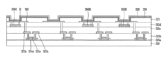
White Organic Light Emitting Diode Display Device and Method of Fabricating the Same
PatentActiveUS20120161141A1
Innovation
- A W-OLED display device with a passivation layer made of silicon nitride, featuring holes to expose and remove outgassing from color filters, and a thickness of 1000-5000 Å to prevent wave guiding, along with a method involving curing processes to remove outgases effectively.
Manufacturing Process Optimization for Electrodes
The optimization of manufacturing processes for WOLED electrodes represents a critical pathway to achieving reduced resistance and enhanced conductivity. Current manufacturing techniques often involve vacuum deposition methods, which while effective, present limitations in terms of material utilization efficiency and scalability. Advanced sputtering techniques with precise control over deposition parameters have demonstrated significant improvements in electrode uniformity and conductivity. By optimizing the sputtering power, pressure, and target-to-substrate distance, manufacturers can achieve up to 30% reduction in sheet resistance compared to conventional methods.
Solution-based processing techniques, including inkjet printing and roll-to-roll manufacturing, offer promising alternatives for large-scale, cost-effective electrode production. These methods enable the precise deposition of conductive materials with controlled thickness and pattern definition. Recent advancements in nanoparticle-based inks have shown particular promise, with silver nanoparticle formulations achieving conductivity values approaching 80% of bulk silver after low-temperature sintering processes.
Post-deposition treatments play a crucial role in optimizing electrode performance. Thermal annealing under controlled atmospheres has been demonstrated to significantly reduce interfacial resistance between electrode layers. Laser annealing techniques provide an alternative approach, offering localized heating that minimizes thermal damage to adjacent organic layers while promoting grain growth and reducing defect density in the electrode material.
Surface modification treatments, including plasma cleaning and chemical functionalization, have shown effectiveness in improving adhesion between electrodes and adjacent layers while reducing contact resistance. Oxygen plasma treatment, in particular, has been found to reduce contact resistance by up to 40% in certain electrode configurations by removing surface contaminants and modifying work function.
Composite electrode structures represent another promising direction for manufacturing optimization. Multi-layer architectures combining high-conductivity materials with transparent conducting oxides have demonstrated enhanced performance compared to single-material electrodes. Manufacturing processes that enable precise control over layer thickness and interface quality are essential for realizing the full potential of these composite structures.
Quality control methodologies, including in-line resistance monitoring and optical inspection techniques, are increasingly being integrated into manufacturing workflows. These approaches enable real-time optimization of process parameters and rapid identification of defects, resulting in more consistent electrode performance and higher manufacturing yields.
Environmental Impact of Advanced Electrode Materials
The advancement of electrode materials for WOLED technology brings significant environmental considerations that must be evaluated alongside performance improvements. Traditional electrode materials often contain rare earth elements and precious metals that pose sustainability challenges due to limited global reserves and environmentally damaging extraction processes. The shift toward high-conductivity electrodes with reduced resistance necessitates examining their complete environmental footprint.
Silver nanowire networks, increasingly adopted for their superior conductivity properties, present a mixed environmental profile. While they enable thinner device architectures that reduce material consumption, the production of silver nanowires involves chemical processes that generate hazardous waste. Additionally, the long-term environmental fate of nanomaterials remains incompletely understood, raising concerns about potential bioaccumulation in ecosystems.
Carbon-based alternatives such as graphene and carbon nanotubes offer promising environmental advantages. These materials utilize abundant carbon rather than scarce metals, potentially reducing extraction impacts. However, their production currently requires high energy inputs and often employs harsh chemicals. Ongoing research into green synthesis methods using sustainable precursors and environmentally benign solvents shows promise for reducing these impacts.
Life cycle assessment (LCA) studies reveal that the environmental benefits of advanced electrode materials may outweigh their production impacts when considering device longevity and efficiency. High-conductivity electrodes extend WOLED operational lifetimes and improve energy efficiency, reducing electronic waste and energy consumption over the product lifecycle. This highlights the importance of evaluating environmental impacts holistically rather than focusing solely on material production.
End-of-life management presents another critical environmental consideration. The complex composition of advanced electrode materials can complicate recycling efforts. Developing specialized recovery processes for valuable materials in these electrodes is essential for closing material loops and minimizing waste. Some promising approaches include selective chemical leaching and advanced separation techniques that can recover precious metals and rare earth elements with high purity.
Regulatory frameworks worldwide are increasingly addressing the environmental implications of advanced materials. The European Union's Restriction of Hazardous Substances (RoHS) directive and similar regulations in other regions are evolving to encompass nanomaterials and novel composites used in electronics. Manufacturers developing high-conductivity WOLED electrodes must anticipate these regulatory trends and design materials with compliance in mind.
Unlock deeper insights with Patsnap Eureka Quick Research — get a full tech report to explore trends and direct your research. Try now!
Generate Your Research Report Instantly with AI Agent
Supercharge your innovation with Patsnap Eureka AI Agent Platform!