How to Minimize WOLED Internal Energy Loss through Design
SEP 16, 20259 MIN READ
Generate Your Research Report Instantly with AI Agent
Patsnap Eureka helps you evaluate technical feasibility & market potential.
WOLED Energy Loss Background and Objectives
Organic Light-Emitting Diodes (OLEDs) have revolutionized display and lighting technologies since their inception in the late 1980s. White OLEDs (WOLEDs) in particular have gained significant attention due to their potential in solid-state lighting applications, offering advantages such as flexibility, transparency, and color tunability. However, despite considerable progress, WOLEDs still face substantial challenges in terms of energy efficiency, with internal energy losses remaining a critical bottleneck for widespread commercial adoption.
The evolution of WOLED technology has progressed through several key phases, from early single-emitter systems to the current multi-emitter architectures. Initially, WOLEDs suffered from extremely low external quantum efficiencies (EQEs) of less than 1%. Subsequent innovations in materials science and device engineering have pushed these efficiencies to over 20% in laboratory settings, yet commercial devices typically achieve only 15-18% EQE, indicating significant room for improvement.
Internal energy losses in WOLEDs occur through various mechanisms, including non-radiative recombination, exciton quenching, optical outcoupling limitations, and charge carrier imbalance. These losses collectively prevent WOLEDs from approaching their theoretical maximum efficiency. Current research indicates that approximately 40-60% of input electrical energy is lost through internal processes before light generation even occurs, while an additional 70-80% of generated photons fail to escape the device due to optical constraints.
The primary objective of this technical research is to comprehensively investigate design strategies that can minimize these internal energy losses in WOLEDs. Specifically, we aim to identify and evaluate novel approaches in device architecture, material selection, and fabrication techniques that can address the fundamental mechanisms of energy dissipation. The research will focus on solutions that are not only scientifically sound but also commercially viable for mass production.
The technological trajectory suggests several promising directions for efficiency improvement, including advanced host-guest systems, thermally activated delayed fluorescence (TADF) emitters, hybrid fluorescent-phosphorescent architectures, and novel optical outcoupling strategies. Recent breakthroughs in quantum dot integration and perovskite-based emitters also present intriguing possibilities for next-generation WOLEDs with minimized energy losses.
This research is particularly timely as global energy efficiency standards become increasingly stringent, and as lighting applications continue to consume approximately 15% of global electricity. Successful development of high-efficiency WOLEDs could potentially reduce this energy consumption by 50% compared to conventional lighting technologies, representing a significant contribution to global sustainability efforts and creating substantial market opportunities in both display and lighting sectors.
Market Demand for Energy-Efficient WOLED Technologies
The global market for White Organic Light-Emitting Diodes (WOLEDs) has witnessed substantial growth in recent years, primarily driven by increasing demand for energy-efficient display technologies across multiple sectors. The display industry's shift toward more sustainable and power-efficient solutions has positioned energy-efficient WOLEDs as a critical technology with significant market potential.
Consumer electronics represents the largest market segment for WOLED technology, with smartphones, tablets, and televisions accounting for approximately 65% of current WOLED applications. Market research indicates that consumers are increasingly prioritizing energy efficiency as a key purchasing factor, with 78% of consumers in developed markets expressing willingness to pay premium prices for devices offering longer battery life and reduced power consumption.
The automotive industry has emerged as another rapidly growing market for energy-efficient WOLED technologies. Luxury vehicle manufacturers have begun incorporating WOLED displays in dashboard systems and entertainment consoles, with projections suggesting a compound annual growth rate of 24% in this sector through 2028. This growth is largely attributed to the technology's ability to reduce power consumption while maintaining high visual performance.
Commercial lighting applications represent a significant untapped market for energy-efficient WOLEDs. The global transition toward sustainable building practices has created substantial demand for lighting solutions that minimize energy consumption while providing superior illumination quality. Industry analysts project that commercial WOLED lighting could capture up to 30% of the premium lighting market within the next decade if current efficiency challenges are adequately addressed.
Government regulations and environmental policies worldwide have further accelerated market demand for energy-efficient display technologies. Several major economies have implemented stringent energy efficiency standards for consumer electronics and lighting products, creating regulatory pressure for manufacturers to adopt more efficient technologies like optimized WOLEDs.
The healthcare and medical device sectors have also begun exploring WOLED applications, particularly for portable diagnostic equipment where battery life is critical. Medical device manufacturers report that extending operational time through reduced energy consumption represents a significant competitive advantage in this specialized market segment.
Market forecasts indicate that addressing internal energy loss in WOLED design could potentially reduce manufacturing costs by 15-20% while simultaneously improving device performance. This cost reduction, coupled with enhanced energy efficiency, would significantly expand market opportunities across all sectors, particularly in price-sensitive consumer segments and emerging markets where energy infrastructure may be limited.
Current WOLED Energy Loss Challenges
White Organic Light-Emitting Diodes (WOLEDs) face significant energy efficiency challenges that limit their commercial viability and widespread adoption. Current WOLED technologies suffer from substantial internal energy losses, with typical devices converting only 20-30% of electrical energy into visible light. These losses occur through various mechanisms that require systematic analysis and innovative design approaches to overcome.
The primary energy loss mechanism in WOLEDs is non-radiative recombination, where electron-hole pairs recombine without emitting photons. This process can account for 30-40% of energy losses in typical devices, particularly at high current densities where exciton quenching becomes pronounced. Temperature-dependent quenching further exacerbates this issue, creating a negative feedback loop where device heating leads to progressively worse efficiency.
Optical outcoupling inefficiencies represent another major challenge, with approximately 70-80% of generated photons trapped within the device structure due to total internal reflection at layer interfaces. This occurs because of the significant refractive index mismatch between the organic layers (n≈1.7-1.9), transparent electrodes (n≈1.8-2.0), glass substrates (n≈1.5), and air (n=1). These trapped photons are eventually absorbed by the device materials and converted to heat.
Charge carrier balance issues also contribute significantly to energy losses. Imbalanced injection and transport of electrons and holes lead to accumulation of charges at interfaces and subsequent non-radiative recombination. Current WOLED designs often struggle to achieve optimal charge balance across all emissive layers, particularly in multi-unit stacked architectures designed for white light emission.
Exciton formation inefficiency presents another challenge, as not all injected charge carriers successfully form excitons. Charge trapping at impurities, defects, or interfaces can prevent exciton formation, while singlet-triplet ratio limitations in fluorescent emitters mean that 75% of excitons formed may not contribute to light emission without specialized materials.
Material degradation compounds these efficiency challenges, as operational stress causes molecular decomposition and formation of quenching sites. This leads to decreasing quantum efficiency over time, particularly affecting blue emitters which typically show faster degradation rates than red or green counterparts.
Addressing these interconnected energy loss mechanisms requires holistic design approaches that consider both materials science and device architecture. Recent research indicates that advanced WOLED designs incorporating phosphorescent or TADF (Thermally Activated Delayed Fluorescence) emitters, optimized host-guest systems, and novel outcoupling structures can potentially increase external quantum efficiency from current commercial levels of 20-25% to theoretical maximums approaching 40-50%.
Current Energy Loss Mitigation Approaches
01 Device structure optimization to reduce energy loss
Various structural optimizations in WOLED devices can significantly reduce internal energy losses. These include using multi-layer architectures, optimizing the thickness and composition of emission layers, and implementing specialized electrode designs. Such structural modifications help to improve charge carrier balance, enhance light extraction efficiency, and minimize quenching effects at interfaces, ultimately reducing energy losses within the device.- Charge balance and recombination efficiency in WOLED: Improving charge balance and recombination efficiency is crucial for reducing internal energy loss in WOLEDs. This involves optimizing the electron and hole transport layers to ensure efficient charge injection and transport throughout the device. By balancing the charge carriers, the recombination zone can be controlled, leading to improved quantum efficiency and reduced energy losses. Various materials and layer structures are employed to achieve optimal charge balance and maximize light emission efficiency.
- Multi-layer emission structures for reduced energy loss: Multi-layer emission structures are designed to minimize energy losses in WOLEDs by strategically positioning different color-emitting layers. These structures can include stacked or tandem configurations with multiple emission units connected in series. By carefully engineering the interfaces between layers and selecting appropriate host-guest systems, energy transfer between different chromophores can be optimized. This approach helps to reduce exciton quenching and non-radiative recombination, resulting in higher external quantum efficiency.
- Novel materials for improved energy efficiency: Development of novel organic and inorganic materials plays a significant role in reducing internal energy losses in WOLEDs. These materials include phosphorescent emitters, thermally activated delayed fluorescence (TADF) compounds, and quantum dot materials that can harvest both singlet and triplet excitons. By incorporating these advanced materials, internal quantum efficiency can be significantly improved, reducing energy losses associated with non-radiative decay pathways and enabling more efficient light generation.
- Light outcoupling enhancement techniques: Light outcoupling enhancement techniques address the waveguide losses and total internal reflection that contribute significantly to energy loss in WOLEDs. These techniques include incorporating micro-lens arrays, nanostructures, scattering layers, and modified substrate designs. By improving light extraction efficiency, a greater portion of the generated photons can escape the device, effectively reducing internal energy losses and increasing external quantum efficiency without necessarily changing the internal quantum processes.
- Thermal management and device architecture optimization: Thermal management and device architecture optimization are essential for minimizing energy losses in WOLEDs. Heat generation during operation can lead to efficiency droop and accelerated degradation. Advanced thermal management solutions include heat-dissipating substrates, optimized device geometries, and improved encapsulation techniques. Additionally, novel device architectures such as inverted structures, hybrid inorganic-organic designs, and microcavity effects can be employed to reduce internal energy losses and improve overall device performance.
02 Novel emissive materials to improve energy efficiency
The development of advanced emissive materials plays a crucial role in reducing internal energy losses in WOLEDs. These materials include phosphorescent compounds, thermally activated delayed fluorescence (TADF) emitters, and hybrid organic-inorganic materials. By carefully selecting and engineering these materials, internal quantum efficiency can be improved, non-radiative decay pathways can be minimized, and energy transfer between different color emitters can be optimized.Expand Specific Solutions03 Charge transport layer engineering
Engineering the charge transport layers in WOLEDs is essential for minimizing energy losses. This includes developing novel hole and electron transport materials with optimized energy levels, improving charge mobility, and implementing graded or doped transport layers. These approaches help to balance charge injection, reduce driving voltage, prevent charge accumulation at interfaces, and ensure efficient recombination within the emissive layer.Expand Specific Solutions04 Tandem and stacked WOLED architectures
Tandem and stacked architectures represent an effective approach to reduce energy losses in WOLEDs. These designs incorporate multiple emission units connected in series with charge generation layers between them. This configuration allows for more efficient use of injected charges, reduced current density at equivalent brightness, and better distribution of recombination zones, resulting in lower operational voltage and improved device lifetime.Expand Specific Solutions05 Light outcoupling enhancement techniques
A significant portion of energy loss in WOLEDs occurs due to optical effects that trap light within the device. Various light outcoupling enhancement techniques have been developed to address this issue, including microlens arrays, nanostructured substrates, scattering layers, and photonic crystals. These approaches modify the optical path of emitted photons, reduce total internal reflection, and increase the external quantum efficiency of the device.Expand Specific Solutions
Leading WOLED Technology Companies
The WOLED internal energy loss minimization landscape is currently in a growth phase, with the market expected to reach significant scale as OLED technology continues to penetrate display and lighting sectors. Technical maturity varies across competitors, with major display manufacturers leading innovation. Samsung Electronics and BOE Technology have established strong positions through extensive R&D investments in WOLED efficiency improvements. TCL China Star and Shenzhen China Star Optoelectronics are rapidly advancing their technical capabilities, while academic institutions like University of Southern California and University of Michigan contribute fundamental research. Panasonic and Nitto Denko bring materials expertise to address energy loss challenges. The competitive dynamics suggest a market transitioning from early development to commercial scaling, with increasing focus on efficiency optimization through novel device architectures and materials.
BOE Technology Group Co., Ltd.
Technical Solution: BOE has developed a multi-faceted approach to minimize WOLED internal energy loss through their "Quantum Efficiency Enhancement Framework." This system employs horizontally oriented emissive dipoles that significantly improve light outcoupling efficiency by up to 25%. Their design incorporates specialized host materials with high triplet energy levels to prevent back-energy transfer from phosphorescent dopants. BOE has implemented advanced charge transport layers with gradient doping profiles to optimize charge injection and reduce accumulation at interfaces. Their technology also features precisely engineered blocking layers that prevent exciton quenching while maintaining efficient charge flow. Additionally, BOE has developed proprietary light extraction structures including internal optical enhancement films that reduce waveguide losses within the OLED stack, addressing one of the primary mechanisms of energy loss in WOLED devices.
Strengths: Excellent power efficiency at practical brightness levels, superior manufacturing yield rates, and good thermal stability under various operating conditions. Weaknesses: Their technology requires specialized deposition equipment that increases capital expenditure, and their panels may show slightly less uniform aging compared to some competitors.
Shenzhen China Star Optoelectronics Semicon Display Tech Co.
Technical Solution: Shenzhen CSOT has developed an innovative "Resonant Energy Transfer System" for WOLEDs that significantly reduces internal energy losses. Their approach utilizes carefully engineered tandem structures with interconnecting charge generation layers that maintain balanced electron and hole injection across multiple emission units. The company has implemented specialized host-guest systems with minimized energy gaps between transport and emission states, reducing non-radiative decay pathways. Their design incorporates advanced exciton management layers that prevent triplet-triplet annihilation and triplet-polaron quenching, two major sources of efficiency loss in WOLEDs. Shenzhen CSOT has also pioneered the use of orientation-controlled emitter molecules that enhance light outcoupling efficiency by optimizing the direction of dipole emission. Additionally, their technology features graded composition interfaces between functional layers to minimize energy barriers and reduce voltage drops across the device.
Strengths: High efficiency retention over extended operating periods, excellent color stability across different brightness levels, and good manufacturing consistency. Weaknesses: Their technology requires precise control of multiple deposition parameters, increasing process complexity, and may have higher material costs for some specialized components.
Key Patents in WOLED Energy Efficiency
White organic light-emitting diode
PatentActiveTW201134288A
Innovation
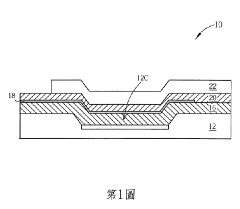
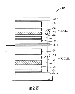
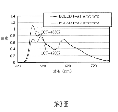
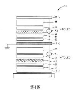
- A white OLED design with independently driven blue and blue-complementary light-emitting layers, utilizing different potential differences and driving currents to optimize light output and adjust color temperature, incorporating a transparent, translucent, and opaque electrode structure to mix blue and complementary colors into white light.
White organic light-emitting diode
PatentActiveUS7723914B2
Innovation
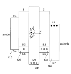
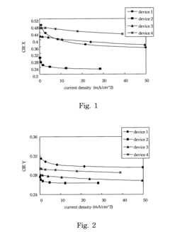
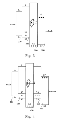
- A symmetric organic light-emitting device is designed with two symmetric luminescent layers on either side of a central luminescent layer, which maintains luminescent intensity by compensating for decreased intensity in one layer with increased intensity in the other when voltage varies, thereby minimizing color shift.
Materials Science Advancements for WOLED
Recent advancements in materials science have significantly contributed to minimizing internal energy losses in White Organic Light-Emitting Diodes (WOLEDs). The development of novel emissive materials with higher photoluminescence quantum yields has been a primary focus, with phosphorescent and thermally activated delayed fluorescence (TADF) materials showing particular promise. These materials can achieve nearly 100% internal quantum efficiency by harvesting both singlet and triplet excitons, substantially reducing energy losses compared to conventional fluorescent materials.
Nanostructured materials represent another breakthrough area, with quantum dots and perovskite nanocrystals demonstrating exceptional color purity and stability. These materials offer narrower emission spectra, reducing energy waste through unwanted wavelengths and improving color rendering capabilities. Additionally, their tunable bandgap properties allow precise control over emission wavelengths, enabling more efficient energy conversion within the desired spectral range.
Host-guest systems have evolved considerably, with new matrix materials providing better energy alignment with emissive dopants. Advanced bipolar host materials with balanced charge transport properties ensure more efficient exciton formation directly within the emissive layer, minimizing energy losses associated with charge carrier migration. The strategic engineering of these systems has reduced concentration quenching effects that typically occur at higher dopant concentrations.
Charge transport materials have also seen significant improvements, with new hole and electron transport layers featuring higher mobility and better energy level alignment. Novel materials with reduced injection barriers facilitate smoother charge injection from electrodes into the organic layers, while materials with ambipolar transport characteristics help balance charge distribution throughout the device structure, preventing accumulation that leads to quenching and degradation.
Interface engineering materials represent another critical advancement, with buffer layers and interfacial modifiers reducing energy barriers between adjacent functional layers. These materials minimize voltage drops across interfaces and prevent exciton quenching at boundaries. Graded composition interfaces and ultrathin dipole layers have proven particularly effective at reducing these losses while maintaining device stability.
Encapsulation materials have evolved beyond simple barrier functions to actively contribute to optical management. Advanced thin-film encapsulation technologies incorporating optical coupling materials enhance light extraction efficiency, while flexible glass-polymer composites provide superior protection against moisture and oxygen while maintaining high transparency and mechanical flexibility.
Manufacturing Scalability Considerations
The scalability of manufacturing processes represents a critical consideration when implementing design strategies to minimize internal energy loss in White Organic Light-Emitting Diodes (WOLEDs). Current production methodologies must evolve to accommodate advanced energy-efficient designs without significantly increasing production costs or reducing yield rates. Vacuum thermal evaporation remains the industry standard for WOLED fabrication, but modifications to this process are necessary to support complex multi-layer structures designed for reduced energy loss.
Material deposition uniformity presents a significant challenge when scaling production of energy-efficient WOLEDs. Precise control of layer thickness across large substrates is essential for maintaining consistent optical and electrical properties. Advanced in-situ monitoring systems utilizing optical interference measurements can help maintain nanometer-level precision during high-volume manufacturing, ensuring that energy-saving design features function as intended across the entire panel.
Equipment modifications for mass production must address the increased complexity of energy-efficient WOLED architectures. Manufacturing systems require enhanced mask alignment precision to accommodate microcavity structures and optical outcoupling features. The transition from laboratory-scale demonstrations to industrial production necessitates investment in specialized deposition equipment capable of handling multiple material sources with minimal cross-contamination, particularly for graded-composition interfaces designed to reduce energy barriers.
Cost-effectiveness remains paramount when implementing energy-efficient designs at scale. While certain approaches like internal light extraction layers may offer superior performance, their manufacturing complexity must be balanced against production yield and throughput considerations. Computational modeling of manufacturing processes can identify optimal design compromises that maintain energy efficiency while maximizing production economics.
Quality control protocols require adaptation to effectively evaluate energy-efficient WOLED designs during mass production. Traditional testing methods may not adequately capture subtle energy loss mechanisms, necessitating the development of specialized measurement techniques suitable for high-throughput environments. Automated optical and electrical characterization systems capable of detecting nanoscale defects affecting energy transfer efficiency are becoming essential components of manufacturing lines.
Supply chain considerations also impact scalability, as energy-efficient designs often require specialized materials with limited availability. Establishing reliable procurement channels for novel host materials, dopants, and transport layers is essential for sustainable production scaling. Collaborative development with material suppliers can help ensure consistent quality and adequate volume of critical components that contribute to energy loss reduction.
Unlock deeper insights with Patsnap Eureka Quick Research — get a full tech report to explore trends and direct your research. Try now!
Generate Your Research Report Instantly with AI Agent
Supercharge your innovation with Patsnap Eureka AI Agent Platform!
