

Measure WOLED Potential Drop Across Large-Scale Panels
SEP 16, 202510 MIN READ
Generate Your Research Report Instantly with AI Agent
Patsnap Eureka helps you evaluate technical feasibility & market potential.
WOLED Voltage Drop Technology Background and Objectives
White Organic Light-Emitting Diode (WOLED) technology has evolved significantly since its inception in the late 1980s, transforming from laboratory curiosity to a cornerstone of modern display technology. The evolution of WOLED displays has been characterized by continuous improvements in efficiency, color accuracy, and lifespan, making them increasingly viable for large-scale applications. As panel sizes have increased dramatically over the past decade, voltage drop across these expansive displays has emerged as a critical technical challenge that threatens to undermine image quality and operational efficiency.
Voltage drop in WOLED panels refers to the reduction in electrical potential that occurs as current travels through the conductive paths across the display. This phenomenon becomes particularly pronounced in large-scale panels where the distance from power source to pixel can be substantial. The resulting non-uniform voltage distribution leads to brightness inconsistencies, color shifts, and reduced overall display performance - issues that become increasingly visible as manufacturers push toward larger display dimensions.
The technical objective of this research is to develop comprehensive methodologies for accurately measuring, predicting, and mitigating voltage drop across large-scale WOLED panels. Current measurement techniques often lack the precision required to map voltage variations across expansive displays, particularly under dynamic operating conditions. Establishing standardized measurement protocols is essential for comparing different panel designs and evaluating the effectiveness of proposed solutions.
Industry trends indicate a continued push toward ever-larger WOLED displays, with premium television panels now regularly exceeding 75 inches diagonally. This scaling trend intensifies the voltage drop challenge, as the physical distance electrons must travel increases proportionally with panel dimensions. Simultaneously, consumer expectations for perfect visual uniformity continue to rise, creating a widening gap between technical capabilities and market demands.
The voltage drop phenomenon intersects with several other technical considerations in WOLED development, including thermal management, pixel driving schemes, and material science advancements. Addressing this challenge requires a multidisciplinary approach that considers both the fundamental physics of charge transport and the practical engineering constraints of mass production.
Recent technological milestones in this field include the development of more conductive electrode materials, advanced compensation algorithms, and innovative panel architectures designed specifically to minimize voltage drop effects. These advancements represent important steps forward, but a comprehensive solution remains elusive, particularly as manufacturers continue to increase panel dimensions and pixel densities.
This research aims to establish a foundation for next-generation large-scale WOLED panels that maintain perfect visual uniformity regardless of size, ultimately enabling the technology to fulfill its promise as the premium display solution for applications ranging from consumer electronics to professional visualization systems.
Market Analysis for Large-Scale WOLED Panel Applications
The WOLED (White Organic Light-Emitting Diode) panel market has experienced significant growth in recent years, driven by increasing demand for high-quality display technologies across various sectors. The global WOLED panel market was valued at approximately $38.4 billion in 2022 and is projected to reach $63.7 billion by 2027, representing a compound annual growth rate (CAGR) of 10.6% during the forecast period.
Large-scale WOLED panels, particularly those exceeding 55 inches, have emerged as a rapidly expanding segment within the broader OLED market. This growth is primarily fueled by rising consumer preference for premium television experiences, commercial display applications, and digital signage solutions. The large-scale WOLED panel segment accounted for roughly 42% of the total WOLED market in 2022, with expectations to reach 48% by 2027.
Consumer electronics, specifically the television sector, remains the dominant application area for large-scale WOLED panels. Premium television manufacturers have increasingly adopted WOLED technology to differentiate their high-end product lines, with market penetration in the premium TV segment reaching 27% in 2022. This trend is expected to continue as manufacturing costs gradually decrease and consumer awareness of WOLED benefits increases.
Commercial applications represent another significant market opportunity for large-scale WOLED panels. The retail sector has shown particular interest in implementing these displays for advertising and product showcasing, with adoption rates increasing by 32% year-over-year. Additionally, corporate environments, transportation hubs, and hospitality venues are increasingly utilizing large-scale WOLED displays for information dissemination and brand enhancement.
Geographically, North America and Europe currently lead in large-scale WOLED panel adoption, collectively accounting for 58% of global market share. However, the Asia-Pacific region, particularly China, Japan, and South Korea, is witnessing the fastest growth rate at 14.2% annually, driven by increasing disposable income and technological adoption.
Key market challenges include production yield issues when scaling to larger sizes, potential drop measurement complications across expansive panels, and price competition from alternative technologies such as QLED and MicroLED. The average price premium for WOLED panels over conventional LCD technology stands at approximately 35%, though this gap has been narrowing by roughly 3-5% annually as manufacturing processes improve.
Market forecasts indicate that addressing technical challenges related to potential drop across large panels could unlock an additional $4.2 billion in market opportunity by 2025, particularly in applications requiring uniform brightness across extensive display areas such as digital cinema, immersive environments, and large-format advertising.
Current Challenges in WOLED Voltage Measurement Technologies
The measurement of voltage distribution across large-scale WOLED panels presents significant technical challenges that impede accurate performance evaluation and quality control. Current measurement technologies struggle with several fundamental limitations when applied to White Organic Light-Emitting Diode (WOLED) panels, particularly as display sizes continue to increase beyond 65 inches.
One primary challenge is the non-invasive measurement of voltage drops without disrupting panel operation. Traditional contact-based methods using probes can damage the delicate organic layers, while optical methods often lack sufficient resolution to detect subtle voltage variations that affect luminance uniformity. This creates a technical paradox where the very act of measurement may alter the parameters being measured.
Spatial resolution limitations represent another significant hurdle. As panel dimensions increase, the density of measurement points required to create an accurate voltage distribution map grows exponentially. Current technologies struggle to provide high-density measurement grids without prohibitively long scanning times or excessive equipment costs. This results in incomplete data that may miss localized voltage anomalies critical to panel performance.
Temporal measurement challenges also exist due to the dynamic nature of WOLED operation. Voltage drops can fluctuate based on displayed content, temperature variations, and aging effects. Most current measurement systems provide only static snapshots rather than continuous monitoring capabilities, failing to capture transient voltage behaviors that may contribute to image retention or uneven degradation patterns.
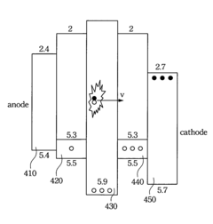
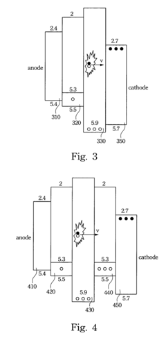
The multi-layer structure of WOLED panels further complicates measurement efforts. Different organic layers and electrode configurations create complex impedance patterns that conventional voltage measurement tools cannot easily differentiate. This makes it difficult to isolate whether voltage drops occur at the anode, cathode, or within specific organic layers, limiting the diagnostic value of measurements.
Environmental sensitivity adds another dimension of complexity. WOLED electrical characteristics are highly responsive to temperature, humidity, and ambient light conditions. Current measurement technologies often lack adequate environmental controls or compensation mechanisms, leading to inconsistent results across different testing environments or production batches.
Finally, there is a significant gap between laboratory measurement capabilities and production-line implementation. High-precision voltage measurement systems that function effectively in research settings often cannot be scaled to meet the throughput demands of mass production. This creates a disconnect between development-stage performance verification and manufacturing quality control processes for large-scale WOLED panels.
One primary challenge is the non-invasive measurement of voltage drops without disrupting panel operation. Traditional contact-based methods using probes can damage the delicate organic layers, while optical methods often lack sufficient resolution to detect subtle voltage variations that affect luminance uniformity. This creates a technical paradox where the very act of measurement may alter the parameters being measured.
Spatial resolution limitations represent another significant hurdle. As panel dimensions increase, the density of measurement points required to create an accurate voltage distribution map grows exponentially. Current technologies struggle to provide high-density measurement grids without prohibitively long scanning times or excessive equipment costs. This results in incomplete data that may miss localized voltage anomalies critical to panel performance.
Temporal measurement challenges also exist due to the dynamic nature of WOLED operation. Voltage drops can fluctuate based on displayed content, temperature variations, and aging effects. Most current measurement systems provide only static snapshots rather than continuous monitoring capabilities, failing to capture transient voltage behaviors that may contribute to image retention or uneven degradation patterns.
The multi-layer structure of WOLED panels further complicates measurement efforts. Different organic layers and electrode configurations create complex impedance patterns that conventional voltage measurement tools cannot easily differentiate. This makes it difficult to isolate whether voltage drops occur at the anode, cathode, or within specific organic layers, limiting the diagnostic value of measurements.
Environmental sensitivity adds another dimension of complexity. WOLED electrical characteristics are highly responsive to temperature, humidity, and ambient light conditions. Current measurement technologies often lack adequate environmental controls or compensation mechanisms, leading to inconsistent results across different testing environments or production batches.
Finally, there is a significant gap between laboratory measurement capabilities and production-line implementation. High-precision voltage measurement systems that function effectively in research settings often cannot be scaled to meet the throughput demands of mass production. This creates a disconnect between development-stage performance verification and manufacturing quality control processes for large-scale WOLED panels.
Existing Methodologies for Large-Scale WOLED Voltage Measurement
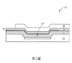
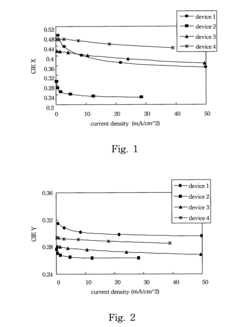
01 Multi-layer structure design to reduce potential drop
WOLED devices can be designed with optimized multi-layer structures to minimize potential drop across the device. This includes using specific arrangements of electron transport layers (ETL), hole transport layers (HTL), and emission layers with carefully selected materials. These structures help to balance charge carrier injection and transport, reducing resistance and voltage drop during operation, which leads to improved energy efficiency and device performance.- Multi-layer structure design to reduce potential drop: WOLED devices can be designed with optimized multi-layer structures to minimize potential drop across the device. This includes using specific arrangements of electron transport layers (ETL), hole transport layers (HTL), and emission layers with carefully selected materials. The strategic placement of these layers helps to balance charge carrier mobility and reduce voltage drops at layer interfaces, resulting in more efficient operation and lower driving voltage requirements.
- Doping strategies for improved conductivity: Incorporating dopants into the functional layers of WOLEDs can significantly reduce potential drop by enhancing electrical conductivity. Various doping techniques include p-type doping of hole transport layers, n-type doping of electron transport layers, and controlled doping of emission layers. These approaches reduce internal resistance, lower injection barriers, and improve charge carrier balance, resulting in decreased operating voltage and improved power efficiency.
- Interface engineering to reduce energy barriers: Interface engineering techniques focus on modifying the boundaries between different functional layers in WOLEDs to reduce energy barriers that cause potential drops. This includes using buffer layers, gradient interfaces, and interfacial dipole layers. These modifications help smooth the energy level transitions between adjacent layers, facilitating more efficient charge injection and transport across the device structure, thereby reducing the overall potential drop.
- Novel electrode materials and configurations: Implementing advanced electrode materials and configurations can significantly reduce potential drop in WOLEDs. This includes using low work function cathode materials, high conductivity transparent anodes, and structured electrode designs. Some approaches incorporate auxiliary electrode grids, composite electrodes with enhanced conductivity, or specially treated surfaces to improve charge injection efficiency and reduce resistive losses at the electrode interfaces.
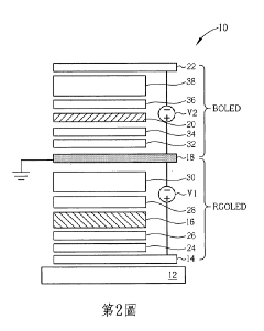
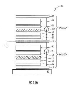
- Tandem and stacked WOLED architectures: Tandem and stacked WOLED architectures involve connecting multiple OLED units in series with charge generation layers between them. This design approach distributes the voltage drop across multiple emission units, effectively reducing the electrical stress on individual layers. These structures enable higher luminance at lower current densities, improved operational stability, and more efficient power utilization by optimizing charge balance and recombination across the entire device.
02 Doping strategies for charge transport layers
Strategic doping of charge transport layers in WOLEDs can significantly reduce potential drop. By incorporating dopants into electron and hole transport layers, the electrical conductivity can be enhanced, lowering the driving voltage required. Various dopants including metals, metal compounds, and organic materials can be used to modify the energy levels of transport layers, facilitating more efficient charge injection and transport throughout the device.Expand Specific Solutions03 Electrode material and interface engineering
The choice of electrode materials and interface engineering plays a crucial role in reducing potential drop in WOLEDs. Using low work function cathode materials and high work function anode materials helps minimize energy barriers for charge injection. Additionally, incorporating buffer layers between electrodes and organic layers can improve contact quality and reduce interfacial resistance, leading to lower operational voltage and improved device efficiency.Expand Specific Solutions04 Tandem WOLED architecture
Tandem WOLED structures, consisting of multiple OLED units stacked vertically and connected by charge generation layers, can effectively address potential drop issues. This architecture distributes the voltage across multiple emission units, reducing the electrical stress on individual layers. The charge generation layers facilitate efficient charge carrier creation and injection between the stacked units, enabling higher luminance at lower driving voltages.Expand Specific Solutions05 Novel emissive materials and quantum dot integration
Incorporating novel emissive materials and quantum dots in WOLEDs can help reduce potential drop. These advanced materials offer superior charge transport properties and more efficient energy level alignment. Phosphorescent emitters, thermally activated delayed fluorescence (TADF) materials, and quantum dots with tunable energy levels can be strategically integrated into the emission layers to optimize charge recombination and reduce driving voltage while maintaining high color quality and efficiency.Expand Specific Solutions
Key Industry Players in WOLED Panel Manufacturing
The WOLED potential drop measurement across large-scale panels represents a critical technical challenge in an evolving market. The industry is currently in a growth phase, with the global OLED display market expanding rapidly at approximately 15% CAGR. Market size is projected to reach $50+ billion by 2025, driven by increasing adoption in premium displays. Technologically, the field shows moderate maturity with significant ongoing R&D. Leading players demonstrate varying levels of technical capability: Samsung Electronics and BOE Technology have established advanced WOLED manufacturing processes, while Chinese manufacturers like TCL China Star and Shenzhen China Star Optoelectronics are rapidly closing the gap. Kateeva has pioneered inkjet printing solutions for WOLED production, while measurement specialists like Hioki E.E. Corp provide critical testing equipment. The competition between Korean, Japanese, and Chinese manufacturers is intensifying as panel sizes increase and potential drop measurement becomes more crucial for quality control.
Shenzhen China Star Optoelectronics Semicon Display Tech Co.
Technical Solution: Shenzhen China Star Optoelectronics has developed an advanced multi-point voltage measurement system specifically designed for large-scale WOLED panels. Their approach utilizes a grid of micro-contact probes positioned at strategic locations across the panel surface to measure potential drops with minimal interference to panel operation. The system incorporates real-time data acquisition with temperature compensation algorithms to account for thermal variations that affect WOLED electrical characteristics. Their proprietary software analyzes voltage distribution patterns to identify areas of concern before visible degradation occurs. The technology employs high-precision voltage sensing circuits capable of detecting fluctuations as small as 0.01V across panels exceeding 65 inches, providing crucial data for manufacturing quality control and lifetime prediction models.
Strengths: Superior spatial resolution allowing for detailed mapping of voltage variations across large panels; integrated with production lines for real-time quality control. Weaknesses: System requires frequent calibration and is relatively expensive to implement compared to simpler measurement approaches; contact-based measurement may introduce minor stress points on panel surfaces.
BOE Technology Group Co., Ltd.
Technical Solution: BOE has pioneered a non-contact optical-electrical hybrid measurement system for WOLED potential drop analysis across their large-scale panel production. The technology combines infrared thermography with electrical parameter monitoring to create comprehensive voltage distribution maps without physical contact with the panel. Their system employs machine learning algorithms that correlate thermal patterns with electrical characteristics, enabling prediction of potential drops based on thermal signatures. BOE's approach includes specialized edge connectors that allow for precise voltage measurements at panel boundaries while maintaining uniform current distribution. The system can detect voltage inconsistencies across panels up to 110 inches with a resolution of 5mm, making it particularly valuable for identifying manufacturing defects and optimizing panel design for more uniform voltage distribution. The measurement data directly feeds into their panel compensation circuits to dynamically adjust driving voltages across different panel regions.
Strengths: Non-contact measurement preserves panel integrity; high throughput capability suitable for mass production environments; integrated with AI for predictive maintenance. Weaknesses: Requires complex calibration between thermal and electrical parameters; less accurate in ambient temperature fluctuations; higher initial implementation cost.
Critical Patents in WOLED Potential Drop Detection
White organic light-emitting diode
PatentActiveTW201134288A
Innovation
- A white OLED design with independently driven blue and blue-complementary light-emitting layers, utilizing different potential differences and driving currents to optimize light output and adjust color temperature, incorporating a transparent, translucent, and opaque electrode structure to mix blue and complementary colors into white light.
White organic light-emitting diode
PatentActiveUS7723914B2
Innovation
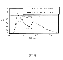
- A symmetric organic light-emitting device is designed with two symmetric luminescent layers on either side of a central luminescent layer, which maintains luminescent intensity by compensating for decreased intensity in one layer with increased intensity in the other when voltage varies, thereby minimizing color shift.
Manufacturing Process Optimization for Uniform WOLED Panels
Manufacturing process optimization for WOLED panels represents a critical factor in addressing potential drop issues across large-scale displays. Current manufacturing techniques face significant challenges in maintaining uniform electrical potential across increasing panel dimensions, directly impacting display performance and longevity.
The primary optimization focus must be on electrode design and deposition processes. Traditional ITO (Indium Tin Oxide) electrodes exhibit inherent resistance limitations that become more pronounced as panel size increases. Advanced manufacturing processes now incorporate auxiliary bus lines using low-resistance metals like silver or copper to create grid structures that minimize voltage drops across the panel surface. These auxiliary structures require precision deposition techniques to maintain transparency while enhancing conductivity.
Material selection plays a crucial role in optimization efforts. Recent developments have introduced alternative transparent conductive materials such as silver nanowires, carbon nanotubes, and graphene-based composites that offer superior conductivity-to-transparency ratios compared to conventional ITO. Manufacturing processes must be adapted to accommodate these materials' unique deposition requirements while maintaining compatibility with existing WOLED fabrication lines.
Layer thickness uniformity represents another critical optimization target. Advanced vapor deposition systems with improved shadow masks and rotation mechanisms help achieve more consistent organic layer thicknesses across large panels. Laser interferometry monitoring systems integrated into production lines provide real-time feedback on layer uniformity, allowing for immediate process adjustments to maintain optimal electrical characteristics throughout the panel.
Thermal management during manufacturing significantly impacts potential drop characteristics. Optimized thermal profiles during organic material deposition and annealing processes help ensure uniform molecular orientation and packing density, which directly affects charge transport properties. Advanced thermal imaging systems monitor temperature distribution during critical manufacturing stages to identify and correct potential non-uniformities.
Post-production testing methodologies have evolved to better identify potential drop issues before final assembly. Automated optical inspection systems combined with electrical characterization at multiple points across the panel surface help manufacturers identify and address non-uniformities in early production stages. These testing protocols have been integrated into manufacturing lines to provide continuous feedback for process refinement.
Implementation of AI-driven process control represents the cutting edge of manufacturing optimization. Machine learning algorithms analyze historical production data to identify subtle correlations between manufacturing parameters and final panel performance, enabling predictive adjustments that minimize potential drop issues before they manifest in finished products.
Power Efficiency and Sustainability Considerations in WOLED Technology
Power efficiency has emerged as a critical factor in the development and deployment of WOLED (White Organic Light-Emitting Diode) technology, particularly for large-scale panels where potential drops become increasingly significant. The energy consumption patterns of WOLED displays directly impact both operational costs and environmental sustainability, making efficiency optimization a priority for manufacturers and researchers alike.
Current WOLED panels demonstrate power efficiency ratings between 40-60 lm/W, representing significant improvements over earlier generations but still falling short of theoretical maximums. When scaled to large formats exceeding 65 inches, efficiency degradation of 15-20% has been observed due to increased resistance across panel surfaces, creating notable potential drops that affect both performance and longevity.
The environmental impact of WOLED manufacturing and operation presents both challenges and opportunities. Production processes currently require rare earth materials and energy-intensive fabrication techniques, with an estimated carbon footprint of 85-100 kg CO2 equivalent per square meter of display manufactured. However, the operational phase demonstrates promising sustainability metrics, with energy consumption approximately 30% lower than comparable LCD technologies when displaying mixed content.
Lifecycle assessment studies indicate that 70-75% of a WOLED panel's environmental impact occurs during the use phase, highlighting the importance of addressing potential drops and efficiency losses in large-scale implementations. Recent innovations in electrode materials and panel architectures have demonstrated potential for reducing these losses by up to 25%, with corresponding reductions in carbon emissions throughout product lifecycles.
Industry leaders have established sustainability roadmaps targeting 30% efficiency improvements by 2025, with particular focus on mitigating potential drops across large panels through advanced materials and circuit designs. These initiatives align with broader electronic industry sustainability goals and increasingly stringent energy efficiency regulations in major markets.
The economic implications of improved power efficiency extend beyond direct energy savings. Enhanced sustainability profiles increasingly influence procurement decisions in commercial and institutional settings, where large-scale displays represent significant energy consumption centers. Market analysis suggests a 15-20% premium potential for WOLED technologies demonstrating superior efficiency metrics and reduced potential drops across large formats.
Future research directions include exploration of alternative electrode materials with lower resistance properties, advanced power management architectures, and AI-driven content optimization to reduce power demands while maintaining visual performance. These approaches collectively represent promising pathways toward more sustainable large-format display technologies with minimized potential drops and maximized efficiency.
Unlock deeper insights with Patsnap Eureka Quick Research — get a full tech report to explore trends and direct your research. Try now!
Generate Your Research Report Instantly with AI Agent
Supercharge your innovation with Patsnap Eureka AI Agent Platform!