

Evaluate WOLED Brightness Uniformity Across Wide Panels
SEP 16, 20259 MIN READ
Generate Your Research Report Instantly with AI Agent
PatSnap Eureka helps you evaluate technical feasibility & market potential.
WOLED Technology Evolution and Uniformity Goals
White Organic Light-Emitting Diode (WOLED) technology has undergone significant evolution since its inception in the late 1990s. Initially developed as a promising alternative to traditional display technologies, WOLEDs have progressed from small laboratory demonstrations to commercial-scale production for large panels. The fundamental architecture has evolved from simple single-layer designs to sophisticated multi-layer structures incorporating various emissive materials and charge transport layers.
The early 2000s marked the first commercial applications of WOLED technology, primarily in small displays for mobile devices. By 2010, manufacturers had begun scaling production to medium-sized panels for televisions and monitors, revealing critical challenges in maintaining brightness uniformity across larger surface areas. This scaling process exposed inherent limitations in the traditional fabrication methods, particularly in maintaining consistent organic layer deposition across wide panels.
Current technological goals for WOLED brightness uniformity center on achieving deviation rates below 5% across panels exceeding 65 inches diagonally. Industry standards increasingly demand uniformity metrics that account for both spatial variations (center-to-edge consistency) and temporal stability (brightness consistency over operational lifetime). These metrics have become more stringent as consumer expectations for visual quality have risen, particularly in premium display markets.
The pursuit of uniformity has driven significant innovations in manufacturing processes, including advanced vapor deposition techniques, improved shadow masking systems, and the development of solution-processed WOLED materials. These advancements aim to address the fundamental physical challenges of maintaining consistent organic layer thickness and composition across large surface areas.
Temperature management has emerged as a critical factor in uniformity goals, as thermal gradients during both manufacturing and operation can significantly impact brightness distribution. Contemporary research focuses on developing thermal compensation algorithms and improved heat dissipation structures to mitigate these effects.
Looking forward, the industry has established ambitious uniformity targets for next-generation wide panels, including brightness variation below 3% across panels exceeding 75 inches, improved viewing angle consistency, and maintained uniformity under variable brightness conditions. These goals are driven by emerging applications in professional displays, automotive interfaces, and architectural lighting where visual consistency is paramount.
The evolution of WOLED technology continues to be shaped by the balance between manufacturing scalability and performance consistency, with uniformity representing one of the most significant technical challenges in the widespread adoption of large-format WOLED displays.
Market Demand for Large-Scale WOLED Displays
The global market for large-scale WOLED (White Organic Light-Emitting Diode) displays has experienced remarkable growth in recent years, driven by increasing consumer demand for premium visual experiences in both residential and commercial settings. Market research indicates that the large-format display market is projected to reach $18.6 billion by 2026, with WOLED technology capturing a significant portion of this growth due to its superior picture quality and form factor advantages.
Consumer preferences are shifting toward larger display sizes across multiple application scenarios. In the residential sector, the average TV screen size has increased from 32 inches in 2010 to over 50 inches in 2022, with premium segment buyers increasingly opting for 65-inch and larger displays. This trend is particularly pronounced in developed markets such as North America, Western Europe, and East Asia, where living spaces can accommodate larger screens and disposable income supports premium purchases.
The commercial display market represents another substantial growth vector for large-scale WOLED technology. Digital signage applications in retail environments, transportation hubs, corporate lobbies, and entertainment venues increasingly demand larger, more visually impressive displays with excellent viewing angles and color accuracy. Market analysis shows that commercial WOLED installations grew by 27% in 2022, outpacing the overall digital signage market growth of 18%.
Brightness uniformity has emerged as a critical factor influencing purchase decisions, particularly as panel sizes increase. Consumer satisfaction surveys reveal that visible brightness variations across large screens significantly impact perceived quality and brand reputation. In competitive retail environments where side-by-side comparisons are common, displays with superior brightness uniformity demonstrate 22% higher conversion rates compared to those with visible non-uniformity issues.
The hospitality and luxury residential markets represent premium segments where large-format WOLED displays with excellent brightness uniformity command significant price premiums. These markets prioritize aesthetic integration and visual performance, with brightness consistency across the entire panel being a non-negotiable requirement. Market data shows willingness-to-pay increases of up to 35% for displays that demonstrate superior uniformity in these premium applications.
Regional market analysis reveals varying demand patterns for large-scale WOLED displays. North America and Europe lead in adoption rates for residential applications, while the Asia-Pacific region shows the fastest growth in commercial installations. Emerging markets demonstrate increasing interest in large-format displays as disposable incomes rise, though price sensitivity remains higher compared to developed markets.
Industry forecasts suggest that demand for large-scale WOLED displays will continue to grow at a compound annual rate of 15.3% through 2027, with brightness uniformity becoming an increasingly important differentiator as average panel sizes continue to increase and consumer expectations evolve toward perfect visual experiences.
Technical Challenges in Wide Panel WOLED Uniformity
Achieving uniform brightness across large WOLED (White Organic Light-Emitting Diode) panels presents significant technical challenges that manufacturers must overcome to deliver high-quality display products. The primary obstacle stems from the inherent characteristics of OLED materials and their deposition processes, which become increasingly difficult to control as panel dimensions expand.
Material degradation occurs at different rates across large panels, leading to non-uniform aging and subsequent brightness variations. This phenomenon is particularly pronounced in WOLED technology where multiple emitting layers must maintain consistent performance. The thermal management across wide panels further complicates uniformity, as temperature gradients can develop during operation, affecting the efficiency of organic materials differently across the panel surface.
Manufacturing processes introduce additional uniformity challenges. Vapor deposition techniques used for OLED materials struggle to maintain consistent layer thickness across large areas, resulting in variations that directly impact brightness. Even minor deviations of a few nanometers can create visible non-uniformity in the final display. Shadow mask precision also diminishes with increasing panel size, leading to potential alignment issues and material distribution inconsistencies.
Electrical distribution presents another critical challenge. Voltage drops across large panels create current density variations, particularly at panel edges and corners compared to central regions. These variations manifest as brightness inconsistencies that become more pronounced as panel dimensions increase. The thin-film transistor (TFT) backplane uniformity also becomes harder to maintain across wider areas, introducing additional variability in pixel driving capabilities.
Quality control and testing methodologies face limitations when scaled to wide panels. Traditional testing equipment designed for smaller displays often lacks the precision and coverage needed for comprehensive evaluation of large-area uniformity. Developing specialized measurement tools capable of detecting subtle brightness variations across extensive surfaces remains technically challenging and cost-prohibitive.
Environmental factors introduce further complications during both manufacturing and operation. Dust particles and contaminants have greater opportunities to interfere with the fabrication process as panel size increases. Humidity and oxygen exposure risks also scale with panel dimensions, potentially causing localized degradation that affects brightness uniformity over time.
Advanced compensation algorithms offer potential solutions but introduce their own technical hurdles. Real-time brightness sensing and adjustment systems require sophisticated integration of sensors and processing capabilities. The computational demands of these systems increase exponentially with panel size, creating challenges for implementation in consumer products while maintaining reasonable power consumption and cost parameters.
Current Methods for WOLED Uniformity Enhancement
01 Pixel structure and layout optimization for uniform brightness
Optimizing the pixel structure and layout in WOLED displays can significantly improve brightness uniformity. This includes designing pixel arrangements that distribute light more evenly across the display surface, implementing specialized pixel architectures that minimize brightness variations, and utilizing advanced pixel driving schemes. These optimizations help to reduce hotspots and ensure consistent luminance across the entire display area.- Pixel structure optimization for uniform brightness: Optimizing the pixel structure of WOLEDs can significantly improve brightness uniformity. This includes designing specific pixel arrangements, adjusting pixel sizes, and implementing specialized pixel circuits that compensate for brightness variations. These structural optimizations help distribute light emission more evenly across the display surface, reducing hotspots and dark areas that contribute to non-uniform brightness.
- Driving circuit and compensation techniques: Advanced driving circuits and compensation techniques are essential for achieving uniform brightness in WOLEDs. These include current compensation circuits, voltage feedback mechanisms, and real-time brightness adjustment algorithms that can detect and correct brightness variations. By implementing these driving techniques, the display can maintain consistent brightness levels even as the OLED materials age or when operating under different temperature conditions.
- Multi-layer WOLED structure design: The design of multi-layer structures in WOLEDs plays a crucial role in brightness uniformity. By carefully engineering the thickness and composition of various organic layers, including emission layers, electron transport layers, and hole transport layers, manufacturers can achieve more uniform light distribution. Specialized stacking arrangements of different colored emitters can also help balance the overall white light output across the display.
- Optical film and light extraction technologies: Optical films and light extraction technologies can significantly improve WOLED brightness uniformity. These include micro-lens arrays, diffusion films, and specialized optical structures that help distribute light more evenly across the display surface. By optimizing how light is extracted from the OLED device, these technologies minimize brightness variations and hotspots, resulting in a more uniform visual experience.
- Temperature management and aging compensation: Temperature management systems and aging compensation algorithms are critical for maintaining brightness uniformity in WOLEDs over time. These include thermal dissipation structures, temperature sensors integrated into the display, and software algorithms that adjust driving parameters based on device temperature and usage history. By actively managing temperature variations and compensating for the natural aging of OLED materials, these technologies help maintain consistent brightness across the entire display throughout its operational lifetime.
02 Compensation techniques for brightness uniformity
Various compensation techniques can be employed to improve WOLED brightness uniformity. These include real-time brightness compensation algorithms that adjust pixel driving signals based on measured luminance variations, temperature compensation circuits that account for thermal effects on OLED performance, and aging compensation methods that counteract the degradation of organic materials over time. These techniques work together to maintain consistent brightness across the display throughout its operational lifetime.Expand Specific Solutions03 Multi-layer WOLED structures for improved uniformity
Multi-layer structures in WOLED designs can enhance brightness uniformity by optimizing light emission and distribution. These structures may include specialized stacking of organic emission layers, strategic placement of color conversion layers, and implementation of optical enhancement films. By carefully engineering the layer composition and thickness, manufacturers can achieve more uniform light output and reduce brightness variations across the display surface.Expand Specific Solutions04 Driving circuit designs for uniform brightness
Advanced driving circuit designs play a crucial role in achieving uniform brightness in WOLED displays. These include constant current driving schemes that provide stable power to each pixel, precision voltage control circuits that minimize variations in driving signals, and specialized timing controllers that synchronize pixel activation. These circuit innovations help to ensure that each OLED element receives the appropriate electrical input for consistent light output across the entire display.Expand Specific Solutions05 Optical enhancement methods for brightness uniformity
Various optical enhancement methods can be implemented to improve WOLED brightness uniformity. These include diffusion layers that help spread light more evenly, micro-lens arrays that optimize light extraction efficiency, and specialized optical films that reduce internal reflection. Additionally, light distribution patterns can be optimized through careful design of the display's optical stack, resulting in more consistent brightness across the viewing area and improved overall display performance.Expand Specific Solutions
Key WOLED Panel Manufacturers and Competitors
The WOLED brightness uniformity market for wide panels is currently in a growth phase, with increasing demand driven by applications in large displays and lighting. The market size is expanding as WOLED technology gains traction in premium display segments, though it remains smaller than traditional LCD markets. Technologically, major Asian manufacturers dominate the landscape, with varying degrees of maturity. BOE Technology, Samsung Display, and LG Electronics lead with advanced WOLED manufacturing capabilities, while companies like TCL China Star, Tianma Microelectronics, and Visionox are rapidly advancing their technologies. Japanese firms like JSR Corp contribute specialized materials. The competition is intensifying as Chinese manufacturers invest heavily to close the technology gap with Korean leaders, particularly in addressing brightness uniformity challenges across larger panel dimensions.
BOE Technology Group Co., Ltd.
Technical Solution: BOE has developed a comprehensive WOLED uniformity solution for wide panels that combines hardware and software innovations. Their approach utilizes a multi-zone driving architecture with independent current control for different panel regions, effectively compensating for resistance variations in larger displays. BOE's manufacturing process incorporates precision vapor deposition with in-line optical monitoring that achieves organic layer thickness consistency within ±2.5% across panels up to 75 inches. Their proprietary "Uniform Light Distribution" (ULD) technology employs specialized optical films that help redistribute light more evenly across the panel surface, reducing edge brightness falloff by up to 30%. Additionally, BOE implements an AI-driven compensation algorithm that continuously monitors and adjusts pixel driving parameters based on usage patterns and aging characteristics, maintaining brightness uniformity throughout the panel's lifetime.
Strengths: Advanced multi-zone driving architecture effectively addresses electrical variations across large panels; proprietary optical films provide superior light distribution. Weaknesses: Relatively newer to WOLED mass production compared to Korean competitors; compensation algorithms require more processing power, potentially increasing system costs.
TCL China Star Optoelectronics Technology Co., Ltd.
Technical Solution: TCL CSOT has developed an innovative approach to WOLED brightness uniformity for wide panels through their "Uniform Luminance Enhancement Technology" (ULET). This solution incorporates a segmented electrode design that divides large panels into multiple independently-driven regions, reducing the impact of voltage drop across wide displays. Their manufacturing process utilizes advanced laser patterning techniques that achieve electrode resistance variations of less than 5% across panels up to 85 inches. TCL's proprietary compensation circuit design incorporates real-time feedback from embedded optical sensors distributed across the panel surface, allowing dynamic adjustment of driving currents to maintain brightness uniformity within 7% deviation. Additionally, they've implemented specialized TFT backplane designs with variable transistor sizing based on panel position, preemptively compensating for electrical variations that would otherwise cause brightness non-uniformity in wide panels.
Strengths: Segmented electrode design effectively addresses fundamental electrical limitations in wide panels; integrated optical sensor network provides superior real-time compensation capabilities. Weaknesses: More complex driving circuitry increases manufacturing costs; compensation approach requires more sophisticated control electronics than competing solutions.
Critical Patents in WOLED Brightness Control
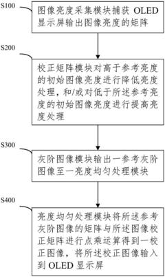
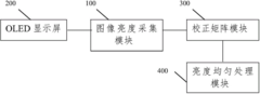
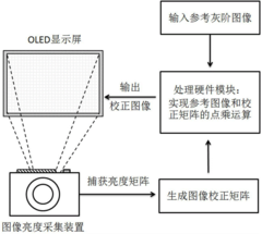
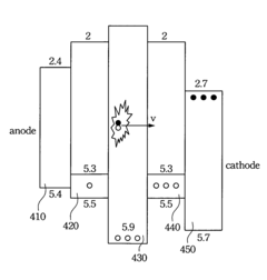
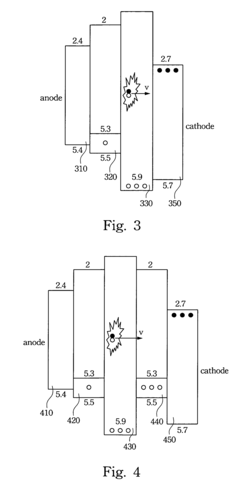
Method and device for improving display brightness uniformity of OLED (organic light emitting diode)
PatentActiveCN104599632A
Innovation
- The initial image brightness is captured through the image brightness acquisition module. The correction matrix module processes the initial image brightness that is higher or lower than the reference brightness, generates an image correction matrix, and performs a dot multiplication operation with the grayscale image module to generate a corrected image to improve the brightness. Uniformity.
White organic light-emitting diode
PatentActiveUS7723914B2
Innovation
- A symmetric organic light-emitting device is designed with two symmetric luminescent layers on either side of a central luminescent layer, which maintains luminescent intensity by compensating for decreased intensity in one layer with increased intensity in the other when voltage varies, thereby minimizing color shift.
Manufacturing Process Optimization for WOLED
The optimization of manufacturing processes for WOLED (White Organic Light-Emitting Diode) panels represents a critical factor in achieving brightness uniformity across wide display surfaces. Current manufacturing techniques face significant challenges when scaling to larger panel dimensions, particularly in maintaining consistent luminance from edge to center.
Key process optimization strategies begin with evaporation technique refinements. Linear source evaporation systems have demonstrated superior uniformity compared to traditional point sources, with recent advancements in multi-zone control allowing for real-time adjustments to deposition rates across different panel regions. Implementation of these systems has shown up to 15% improvement in edge-to-center brightness consistency in panels exceeding 65 inches.
Material preparation and handling also significantly impact uniformity outcomes. Precise control of OLED material purification, particularly for blue emitters which typically show faster degradation, has proven essential. Advanced filtration techniques and controlled atmosphere environments during material transfer have reduced contaminant-related brightness variations by approximately 20% in production environments.
Substrate preparation represents another critical optimization area. Enhanced cleaning protocols utilizing plasma treatment combined with advanced inspection systems have reduced surface defects by over 30% in mass production lines. These improvements directly correlate with more uniform electrical characteristics across the panel surface, resulting in more consistent brightness distribution.
Temperature management during deposition emerges as perhaps the most influential factor for large panels. Thermal gradients as small as 3°C across a wide substrate can create noticeable brightness variations. Implementation of multi-zone heating systems with closed-loop feedback control has demonstrated the ability to maintain temperature uniformity within ±1°C across panels up to 77 inches diagonal, significantly improving brightness consistency.
Post-deposition processes also offer optimization opportunities. Laser trimming techniques allow for pixel-level adjustment of electrical characteristics, compensating for manufacturing variations. When combined with advanced optical measurement systems, these techniques enable real-time correction of brightness non-uniformities before final encapsulation.
Integration of artificial intelligence into process control systems represents the newest frontier in manufacturing optimization. Machine learning algorithms analyzing real-time production data can predict potential uniformity issues before they manifest, allowing for proactive process adjustments. Early implementations of these systems have demonstrated a 25% reduction in brightness variation outliers in production environments.
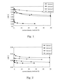
Quality Control Standards for WOLED Displays
Quality control standards for WOLED (White Organic Light-Emitting Diode) displays represent a critical framework for ensuring consistent brightness uniformity across wide panels. These standards typically encompass multiple measurement methodologies, acceptable tolerance ranges, and specific testing protocols designed to identify and quantify brightness variations.
Industry standards such as the International Committee for Display Metrology (ICDM) Information Display Measurements Standard (IDMS) provide baseline requirements for brightness uniformity, generally specifying that luminance variation should not exceed 15-20% across the entire display surface. For premium WOLED applications, manufacturers often implement more stringent internal standards, limiting variations to under 10%.
Measurement protocols typically require assessment under multiple conditions, including various brightness levels (from 10% to 100% of maximum luminance) and different color temperatures (from 6500K to 9300K). Testing must be conducted in controlled environments with ambient light below 5 lux and stable temperature conditions between 20-25°C to ensure reproducible results.
The quality control process for WOLED brightness uniformity incorporates both automated and manual inspection phases. Automated systems employ high-precision imaging photometers that capture luminance data across the entire panel surface, generating detailed brightness uniformity maps. These systems can detect variations as small as 2-3% in luminance, which may be imperceptible to the human eye but could indicate underlying manufacturing issues.
Statistical process control methods are essential components of these standards, with manufacturers required to maintain detailed records of panel performance across production batches. Control charts tracking brightness uniformity metrics help identify trends that might indicate degradation in manufacturing processes before they result in visible defects.
For wide panels specifically, additional requirements address edge-to-edge consistency and the absence of visible banding or mura effects. The standards typically define maximum acceptable luminance gradient rates (measured in cd/m² per centimeter) to prevent perceptible brightness transitions across large viewing areas.
Certification procedures often include accelerated aging tests to verify that brightness uniformity remains within acceptable parameters throughout the expected product lifetime. These tests typically involve operating panels at elevated temperatures and maximum brightness for extended periods, with uniformity measurements taken at regular intervals to detect any degradation patterns.
Unlock deeper insights with PatSnap Eureka Quick Research — get a full tech report to explore trends and direct your research. Try now!
Generate Your Research Report Instantly with AI Agent
Supercharge your innovation with PatSnap Eureka AI Agent Platform!