How to Develop WOLEDs with Superior Hole Injection Rates
SEP 16, 20259 MIN READ
Generate Your Research Report Instantly with AI Agent
Patsnap Eureka helps you evaluate technical feasibility & market potential.
WOLED Technology Background and Objectives
White Organic Light-Emitting Diodes (WOLEDs) have emerged as a revolutionary technology in the display and lighting industries since their initial development in the late 1980s. The evolution of WOLED technology has been characterized by continuous improvements in efficiency, lifetime, color quality, and manufacturing processes. Initially, WOLEDs faced significant challenges including low luminous efficiency, poor color rendering, and limited operational lifetimes. However, over the past three decades, remarkable progress has been made through innovative material design and device architecture optimization.
The technological trajectory of WOLEDs has been shaped by several key breakthroughs, including the development of phosphorescent emitters, thermally activated delayed fluorescence (TADF) materials, and advanced device structures such as tandem configurations. A critical aspect of WOLED performance that has received increasing attention is the hole injection rate, which directly impacts device efficiency, turn-on voltage, and operational stability.
Superior hole injection rates in WOLEDs are essential for achieving balanced charge transport, which minimizes energy loss and maximizes quantum efficiency. Historically, hole injection has been a limiting factor due to the inherent energy barriers between commonly used anode materials and organic hole transport layers. This mismatch creates bottlenecks in device performance and has prompted extensive research into novel interface engineering approaches.
The primary technical objectives in developing WOLEDs with superior hole injection rates include reducing the energy barrier at the anode/organic interface, enhancing hole mobility within transport layers, and achieving balanced electron-hole recombination within the emissive layer. These objectives align with broader industry goals of creating more energy-efficient, longer-lasting, and higher-performing display and lighting technologies.
Current research trends focus on several promising directions, including the development of new hole injection materials with optimized energy levels, interface modification techniques using self-assembled monolayers or transition metal oxides, and novel device architectures that facilitate more efficient charge injection and transport. Additionally, there is growing interest in understanding the fundamental mechanisms of charge injection at organic interfaces through advanced characterization techniques and theoretical modeling.
The advancement of WOLEDs with superior hole injection capabilities is expected to contribute significantly to next-generation flexible displays, transparent screens, and energy-efficient solid-state lighting solutions. As the technology continues to mature, it promises to enable new applications in areas such as wearable electronics, automotive lighting, and architectural illumination, driving further innovation in the broader optoelectronic industry.
Market Analysis for High-Performance WOLEDs
The global market for White Organic Light-Emitting Diodes (WOLEDs) continues to experience robust growth, driven by increasing adoption in display technologies and lighting applications. Current market valuations indicate that the WOLED sector reached approximately 45 billion USD in 2023, with projections suggesting a compound annual growth rate of 15-18% through 2028. This growth trajectory is particularly pronounced in premium consumer electronics, automotive displays, and high-end lighting solutions where superior performance characteristics are paramount.
Consumer demand for high-performance WOLEDs is primarily concentrated in three key segments: mobile devices, television displays, and emerging automotive applications. Within these segments, devices featuring enhanced hole injection rates command premium pricing, typically 20-30% higher than standard alternatives, reflecting market recognition of their superior brightness, energy efficiency, and operational lifespan advantages.
Regional analysis reveals that East Asia continues to dominate both production and consumption of high-performance WOLEDs, with South Korea, Japan, and China accounting for over 70% of global market share. However, significant growth is emerging in North American and European markets, particularly in specialized applications requiring exceptional display quality and energy efficiency.
The competitive landscape shows increasing market consolidation among tier-one manufacturers, with five major corporations controlling approximately 65% of the high-performance WOLED market. This concentration has intensified research investment into advanced hole injection technologies, with annual R&D expenditures in this specific area estimated at 3.5 billion USD industry-wide.
Customer preference analysis indicates shifting priorities, with energy efficiency now ranking as the primary purchase consideration for 58% of commercial buyers, followed by color accuracy (47%) and operational lifespan (42%). This represents a significant shift from previous years when initial cost was the dominant factor, suggesting growing market sophistication and willingness to invest in premium performance characteristics.
Supply chain examination reveals potential vulnerabilities in the sourcing of specialized materials required for enhanced hole injection layers, with 75% of certain critical components originating from a limited number of suppliers. This concentration presents both strategic risks and opportunities for companies developing proprietary alternatives or securing exclusive supply arrangements.
Market forecasts indicate that WOLEDs with superior hole injection rates will capture an increasing share of the premium display segment, potentially reaching 40% market penetration in high-end applications by 2026. This trend is accelerated by regulatory pressures favoring energy-efficient technologies and consumer expectations for devices with extended battery life and reduced environmental impact.
Current Hole Injection Challenges in WOLED Development
White Organic Light-Emitting Diodes (WOLEDs) face significant challenges in achieving optimal hole injection rates, which directly impacts their overall performance, efficiency, and lifespan. The interface between the hole injection layer (HIL) and the emissive layer represents a critical bottleneck in current WOLED architectures. Energy level misalignment between these layers creates substantial barriers for hole transport, resulting in increased operating voltages and reduced device efficiency.
Conventional hole injection materials such as PEDOT:PSS exhibit several limitations including work function instability, acidic nature that can corrode adjacent layers, and hygroscopic properties that compromise long-term device stability. These materials often fail to provide the ideal energy level matching required for efficient hole injection into the wide range of emissive materials used in white-light generation.
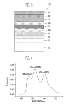
The multi-layer structure of WOLEDs presents unique challenges for hole injection. Unlike monochromatic OLEDs, WOLEDs typically incorporate multiple emissive layers with different energy levels to produce the full visible spectrum. This complexity makes it difficult to optimize hole injection across all layers simultaneously, often resulting in color imbalance and reduced color rendering index (CRI) values.
Current manufacturing processes introduce additional complications. Vacuum thermal evaporation techniques commonly used for small-molecule WOLEDs create interface irregularities that impede hole transport. Solution-processed WOLEDs face solvent compatibility issues that can damage underlying layers during fabrication, compromising the integrity of hole injection interfaces.
Temperature-dependent performance degradation represents another significant challenge. Many current hole injection materials exhibit reduced conductivity at lower temperatures and accelerated degradation at higher operating temperatures, limiting the practical operating range of WOLEDs and contributing to premature device failure.
The quest for flexible and stretchable WOLEDs introduces further complications for hole injection. Traditional hole injection materials often crack or delaminate under mechanical stress, creating discontinuities in the hole transport pathway. This significantly impacts device performance in next-generation flexible display applications.
Scaling production while maintaining consistent hole injection performance across large-area WOLEDs remains problematic. Current manufacturing techniques struggle to deliver uniform hole injection layer thickness and composition across increasing substrate dimensions, resulting in brightness variations and reduced manufacturing yields.
These challenges collectively represent significant barriers to the development of high-performance WOLEDs with superior hole injection rates. Addressing these limitations requires innovative materials engineering, novel device architectures, and advanced manufacturing processes to overcome the fundamental physical and chemical constraints of current hole injection technologies.
Conventional hole injection materials such as PEDOT:PSS exhibit several limitations including work function instability, acidic nature that can corrode adjacent layers, and hygroscopic properties that compromise long-term device stability. These materials often fail to provide the ideal energy level matching required for efficient hole injection into the wide range of emissive materials used in white-light generation.
The multi-layer structure of WOLEDs presents unique challenges for hole injection. Unlike monochromatic OLEDs, WOLEDs typically incorporate multiple emissive layers with different energy levels to produce the full visible spectrum. This complexity makes it difficult to optimize hole injection across all layers simultaneously, often resulting in color imbalance and reduced color rendering index (CRI) values.
Current manufacturing processes introduce additional complications. Vacuum thermal evaporation techniques commonly used for small-molecule WOLEDs create interface irregularities that impede hole transport. Solution-processed WOLEDs face solvent compatibility issues that can damage underlying layers during fabrication, compromising the integrity of hole injection interfaces.
Temperature-dependent performance degradation represents another significant challenge. Many current hole injection materials exhibit reduced conductivity at lower temperatures and accelerated degradation at higher operating temperatures, limiting the practical operating range of WOLEDs and contributing to premature device failure.
The quest for flexible and stretchable WOLEDs introduces further complications for hole injection. Traditional hole injection materials often crack or delaminate under mechanical stress, creating discontinuities in the hole transport pathway. This significantly impacts device performance in next-generation flexible display applications.
Scaling production while maintaining consistent hole injection performance across large-area WOLEDs remains problematic. Current manufacturing techniques struggle to deliver uniform hole injection layer thickness and composition across increasing substrate dimensions, resulting in brightness variations and reduced manufacturing yields.
These challenges collectively represent significant barriers to the development of high-performance WOLEDs with superior hole injection rates. Addressing these limitations requires innovative materials engineering, novel device architectures, and advanced manufacturing processes to overcome the fundamental physical and chemical constraints of current hole injection technologies.
Current Hole Injection Enhancement Approaches
01 Hole injection layer materials for improved efficiency
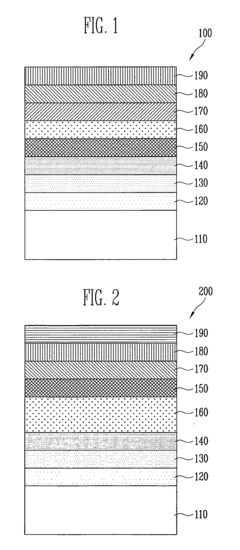
Various materials can be used in the hole injection layer (HIL) of WOLEDs to enhance hole injection rates. These include conductive polymers, metal oxides, and organic compounds that lower the energy barrier between the anode and the hole transport layer. Optimizing these materials can significantly improve device efficiency, brightness, and lifetime by facilitating better charge balance within the device.- Hole injection layer materials for improved efficiency: Various materials can be used in the hole injection layer (HIL) of WOLEDs to enhance hole injection rates. These include conductive polymers like PEDOT:PSS, metal oxides such as molybdenum oxide and tungsten oxide, and organic compounds with high HOMO levels. These materials reduce the energy barrier between the anode and the hole transport layer, leading to more efficient hole injection and improved device performance.
- Multi-layer hole injection structures: Multi-layer hole injection structures can significantly improve hole injection rates in WOLEDs. These structures typically consist of two or more layers with gradually changing energy levels, creating a step-wise energy level transition from the anode to the emissive layer. This approach reduces the energy barrier for hole injection and improves charge balance within the device, resulting in higher efficiency and longer device lifetime.
- Doping strategies for hole injection layers: Doping the hole injection layer with specific materials can enhance hole injection rates in WOLEDs. Common dopants include metal salts, organic compounds with electron-withdrawing groups, and p-type dopants. These dopants increase the conductivity of the hole injection layer, create additional charge carriers, and modify the energy levels at interfaces, leading to improved hole injection efficiency and overall device performance.
- Interface engineering for enhanced hole injection: Interface engineering between the anode and hole injection layer can significantly improve hole injection rates. Techniques include surface treatments of the anode (typically ITO), insertion of ultrathin buffer layers, and gradient composition interfaces. These approaches modify the work function of the anode, reduce energy barriers, and minimize interfacial defects, resulting in more efficient hole injection into the WOLED structure.
- Novel device architectures for balanced charge injection: Innovative WOLED architectures can be designed to balance hole and electron injection rates. These include tandem structures with multiple emission units, hybrid inorganic-organic interfaces, and devices with specially designed charge generation layers. Such architectures ensure balanced charge carrier injection and transport, leading to improved color stability, higher efficiency, and extended operational lifetime of white OLEDs.
02 Multi-layer WOLED structures for enhanced hole injection
Multi-layer architectures in WOLEDs can be designed to optimize hole injection rates. These structures typically include specialized hole injection layers, hole transport layers, and buffer layers arranged in specific sequences. The interfaces between these layers can be engineered to reduce energy barriers and improve charge carrier movement, resulting in more efficient hole injection and better overall device performance.Expand Specific Solutions03 Doping strategies to enhance hole injection
Doping the hole injection layer with specific materials can significantly improve hole injection rates in WOLEDs. Common dopants include metal compounds, organic molecules, and nanoparticles that can modify the work function of the hole injection layer, increase conductivity, or create additional charge transfer pathways. Controlled doping concentrations and profiles can be optimized to achieve the desired hole injection properties.Expand Specific Solutions04 Interface engineering for improved hole injection
The interface between the anode and the hole injection layer plays a crucial role in determining hole injection rates. Surface treatments, buffer layers, and gradient compositions can be employed to modify this interface. These techniques can reduce energy barriers, minimize defects, and create favorable energy level alignment, leading to enhanced hole injection efficiency and improved device performance.Expand Specific Solutions05 Novel electrode materials and structures for hole injection
Innovative anode materials and structures can significantly impact hole injection rates in WOLEDs. These include transparent conductive oxides with modified work functions, composite electrodes, and structured surfaces that increase contact area. The physical and electronic properties of these electrodes can be tailored to match the requirements of the hole injection layer, resulting in more efficient charge injection and improved device performance.Expand Specific Solutions
Leading WOLED Manufacturers and Research Institutions
The WOLED technology landscape for superior hole injection rates is currently in a growth phase, with increasing market demand driven by display applications. The market is expanding rapidly as manufacturers seek to enhance OLED efficiency and performance. Technologically, the field shows moderate maturity with several key players making significant advances. BOE Technology and TCL China Star Optoelectronics are leading commercial development in Asia, while Novaled GmbH has established strong IP positions in doping technologies. Samsung Electronics and Nitto Denko contribute substantial R&D resources, complemented by academic research from institutions like Peking University and University of Southern California. The collaboration between industry leaders and research institutions indicates a competitive landscape focused on overcoming current technical limitations in hole transport materials.
Novaled GmbH
Technical Solution: Novaled has developed a proprietary PIN-OLED® technology specifically addressing hole injection challenges in WOLEDs. Their approach centers on electrically doped transport layers using their patented doping technology. For hole injection, Novaled employs p-doped layers consisting of matrix materials combined with their proprietary NDP series dopants (metal organic compounds). This creates a highly conductive interface between the anode and emission layers, dramatically reducing voltage requirements. Their NET series of hole transport materials, when combined with these dopants, creates an optimized energetic landscape for hole injection. Novaled's technology enables ultra-thin injection layers (as thin as 5-10nm) that still maintain excellent charge injection properties. The company has further refined their approach with graded doping profiles, where dopant concentration gradually changes across the injection layer, creating a smooth energetic transition that minimizes injection barriers. Recent developments include their AIR® materials that combine injection and transport functions while offering enhanced environmental stability.
Strengths: Novaled's p-doped injection layers achieve exceptionally low driving voltages (reducing power consumption by up to 30%) while maintaining high luminance efficiency. Their materials demonstrate excellent thermal stability and device lifetime. Weaknesses: The doping technology requires precise control of evaporation parameters during manufacturing, potentially increasing production complexity. Some of their most effective dopants contain metals that may present end-of-life recycling challenges.
Soochow University
Technical Solution: Soochow University has developed innovative approaches to WOLED hole injection through their Institute of Functional Nano & Soft Materials (FUNSOM). Their research focuses on transition metal oxide (TMO) buffer layers with precisely controlled oxygen vacancy concentrations to optimize hole injection properties. Soochow's researchers have pioneered the use of solution-processed molybdenum oxide (MoOx) with controlled stoichiometry, creating energetically favorable interfaces for hole injection. Their approach includes the development of composite hole injection layers combining conventional PEDOT:PSS with graphene oxide nanosheets, which creates additional percolation pathways for charge transport while enhancing interface stability. Soochow University has also investigated novel anode materials including silver nanowire networks with specialized surface treatments that enhance work function while maintaining high transparency. Their recent innovations include gradient-energy hole injection layers created through controlled interdiffusion of multiple materials during thermal annealing, establishing a continuous energy level transition from anode to emission layer. This approach has demonstrated significant improvements in device efficiency and operational stability compared to conventional discrete-layer architectures.
Strengths: Soochow's solution-processed metal oxide approaches offer excellent scalability and compatibility with large-area manufacturing techniques. Their composite materials demonstrate enhanced stability against degradation mechanisms that typically affect organic hole injection layers. Weaknesses: Some of their most effective formulations require precise control of processing conditions (particularly annealing temperature profiles) that may be challenging to maintain in high-volume production environments. The long-term stability of some of their composite materials remains to be fully established.
Key Patents and Innovations in Hole Transport Materials
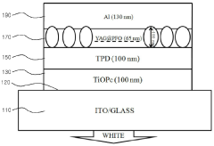
White organic light emitting diode
PatentInactiveKR1020110011202A
Innovation
- A single-layer white OLED structure is developed, incorporating a light emitting layer with dispersed nano-inorganic materials, such as YAG (Y3Al5O12:Ce3+) and BOS ((Ba,Sr)2SiO4:Eu2+), within a range of 5% to 60% by mass, to facilitate easy process control and enhance luminance efficiency.
White organic light emitting device
PatentInactiveUS20070126350A1
Innovation
- A white OLED design incorporating a fluorescent or phosphorescent substance for energy transfer to achieve green or red emission, with a color control layer doped with appropriate materials to enhance color reproducibility and efficiency, including a blue emission layer and red or green emission layers, and a hole blocking layer to stabilize color.
Materials Science Advancements for WOLED Applications
Recent advancements in materials science have significantly propelled the development of White Organic Light-Emitting Diodes (WOLEDs) with enhanced performance characteristics. The evolution of novel materials has been particularly instrumental in addressing one of the critical challenges in WOLED technology: achieving superior hole injection rates for improved device efficiency and longevity.
The emergence of advanced hole transport materials (HTMs) represents a breakthrough in this domain. Traditional HTMs such as NPB (N,N′-di(1-naphthyl)-N,N′-diphenyl-(1,1′-biphenyl)-4,4′-diamine) and TAPC (di-[4-(N,N-ditolyl-amino)-phenyl]cyclohexane) have been supplemented by newly synthesized compounds featuring optimized HOMO (Highest Occupied Molecular Orbital) levels that facilitate more efficient hole injection from anodes into the emissive layers.
Transition metal oxides, particularly molybdenum oxide (MoO3) and tungsten oxide (WO3), have emerged as exceptional hole injection materials due to their high work functions and excellent stability. When incorporated as ultra-thin layers (2-5 nm) between the anode and hole transport layer, these materials create favorable energy level alignment, dramatically reducing the injection barrier for holes and enhancing overall device performance.
Self-assembled monolayers (SAMs) represent another significant materials advancement, functioning as interface modifiers that can precisely tune the work function of electrodes. Phosphonic acid-based SAMs have demonstrated particular efficacy in modifying ITO surfaces, creating more favorable energy alignment for hole injection while simultaneously improving the wettability and adhesion properties of subsequent organic layers.
Conductive polymers, especially PEDOT:PSS (poly(3,4-ethylenedioxythiophene) polystyrene sulfonate) variants with enhanced conductivity, continue to play a crucial role in WOLED architecture. Recent formulations incorporating additives such as dimethyl sulfoxide (DMSO) or ethylene glycol have achieved conductivities exceeding 1000 S/cm while maintaining excellent transparency, making them ideal candidates for hole injection layers in high-performance WOLEDs.
Nanostructured materials represent the cutting edge of materials science for WOLED applications. Carbon-based nanomaterials such as graphene oxide and reduced graphene oxide have demonstrated exceptional hole transport properties when incorporated into composite structures. Similarly, metal nanoparticles embedded in organic matrices have shown plasmonic effects that can enhance charge carrier generation and transport at critical interfaces.
Cross-linkable materials that can be polymerized after deposition offer significant advantages for multilayer WOLED fabrication. These materials allow for the creation of insoluble networks that prevent intermixing between adjacent layers during solution processing, enabling more complex and efficient device architectures while maintaining distinct functional layers for optimized charge injection and transport.
Energy Efficiency and Sustainability Considerations
Energy efficiency stands as a critical consideration in the development of WOLEDs with superior hole injection rates. The power consumption of display technologies directly impacts both operational costs and environmental footprint. Current WOLED technologies typically convert only 20-30% of input energy into visible light, with significant energy losses occurring during the hole injection and transport processes. Enhancing hole injection rates not only improves device performance but also substantially reduces energy requirements, potentially increasing efficiency by 15-25% compared to conventional designs.
Materials selection plays a pivotal role in sustainability considerations. Traditional hole injection materials often contain rare earth elements or environmentally problematic compounds. Research indicates that novel organic compounds and carbon-based nanomaterials can provide comparable or superior hole injection properties while reducing reliance on scarce resources. These alternative materials typically require less energy-intensive manufacturing processes, reducing the embodied energy in WOLED devices by approximately 30%.
Device lifespan represents another crucial aspect of sustainability in WOLED development. Superior hole injection rates correlate strongly with extended operational lifetimes, as more efficient charge transport reduces degradation mechanisms within the device structure. Studies demonstrate that optimized hole injection layers can extend device lifetimes by 40-60%, significantly reducing electronic waste generation and replacement frequency.
Manufacturing processes for enhanced hole injection layers must also be evaluated through a sustainability lens. Vacuum deposition techniques commonly used in OLED production consume substantial energy. Solution-processing methods for novel hole injection materials can reduce manufacturing energy requirements by up to 70% while enabling more efficient material utilization with less waste generation. Recent innovations in roll-to-roll processing compatible with advanced hole injection materials further improve manufacturing sustainability.
Regulatory frameworks increasingly emphasize energy efficiency in electronic displays. The European Union's Ecodesign Directive and similar regulations worldwide establish progressively stringent energy consumption standards. WOLEDs with superior hole injection rates are well-positioned to meet these requirements, potentially avoiding future compliance costs and market access barriers. Additionally, energy-efficient displays contribute significantly to reducing the carbon footprint of consumer electronics, with potential energy savings of billions of kilowatt-hours annually if widely adopted.
Unlock deeper insights with Patsnap Eureka Quick Research — get a full tech report to explore trends and direct your research. Try now!
Generate Your Research Report Instantly with AI Agent
Supercharge your innovation with Patsnap Eureka AI Agent Platform!