

Optimize WOLED Electron Hole Balance for Power Efficiency
SEP 16, 20259 MIN READ
Generate Your Research Report Instantly with AI Agent
Patsnap Eureka helps you evaluate technical feasibility & market potential.
WOLED Technology Background and Efficiency Goals
White Organic Light-Emitting Diodes (WOLEDs) have emerged as a revolutionary technology in the display and lighting industries since their initial development in the late 1980s. The evolution of WOLED technology has been marked by continuous improvements in efficiency, lifetime, and color quality. Originally, OLEDs suffered from poor efficiency and short operational lifespans, but significant advancements in materials science and device architecture have transformed them into viable commercial products.
The fundamental operating principle of WOLEDs involves the recombination of electrons and holes within organic semiconductor materials to produce white light. This process occurs in a multi-layer structure typically consisting of electron transport layers (ETLs), emissive layers (EMLs), and hole transport layers (HTLs) sandwiched between a cathode and an anode. The balance between electron and hole injection and transport is crucial for maximizing device efficiency.
Power efficiency in WOLEDs is quantified through metrics such as external quantum efficiency (EQE), current efficiency (cd/A), and power efficiency (lm/W). Industry benchmarks have evolved rapidly, with state-of-the-art devices now achieving EQEs exceeding 30% and power efficiencies above 100 lm/W under laboratory conditions. Commercial WOLED panels typically operate at 40-70 lm/W, indicating significant room for improvement.
The electron-hole balance represents one of the most critical factors affecting WOLED efficiency. When this balance is optimized, the recombination zone is properly positioned within the emissive layer, maximizing photon generation while minimizing non-radiative losses. Historically, achieving this balance has been challenging due to the inherent mobility differences between electrons and holes in organic semiconductors.
Current efficiency goals for WOLED technology focus on reaching power efficiencies of 120-150 lm/W for commercial lighting applications and 80-100 lm/W for display applications while maintaining color stability and device longevity. These targets are driven by energy efficiency regulations and competition with alternative technologies such as LED lighting.
The technology roadmap for WOLED efficiency improvement includes several parallel approaches: development of new host and dopant materials with improved charge transport properties, optimization of device architectures to enhance charge balance, implementation of optical outcoupling structures to improve light extraction, and refinement of manufacturing processes to ensure consistent performance at scale.
Recent research trends indicate that addressing the electron-hole balance issue could potentially yield efficiency improvements of 20-30% in existing WOLED designs without requiring entirely new materials or radical device redesigns. This represents a particularly attractive approach for near-term efficiency gains in commercial applications.
Market Demand Analysis for High-Efficiency WOLED Displays
The WOLED (White Organic Light-Emitting Diode) display market has experienced significant growth in recent years, driven by increasing demand for high-quality displays with superior energy efficiency. Market research indicates that the global OLED display market is projected to reach $48.8 billion by 2023, with WOLED technology representing a substantial segment of this market due to its superior color reproduction and power efficiency advantages.
Consumer electronics, particularly high-end televisions and premium smartphones, constitute the primary market for WOLED displays. The television segment has shown remarkable adoption rates, with WOLED TVs commanding premium positioning in manufacturers' product lineups. Market penetration in this segment continues to expand as production costs decrease and consumer awareness of WOLED benefits increases.
Energy efficiency has emerged as a critical differentiator in display technologies, with both regulatory pressures and consumer preferences driving demand for more power-efficient solutions. The European Union's eco-design regulations and Energy Star requirements in North America have established increasingly stringent power consumption standards for electronic displays, creating market pull for optimized WOLED technologies that can achieve better electron-hole balance and improved power efficiency.
Commercial applications represent another growing market segment for high-efficiency WOLED displays. Digital signage, retail displays, and hospitality industry applications increasingly demand displays that can operate continuously with minimal power consumption while maintaining excellent visual performance. The reduced operational costs associated with more efficient displays create a compelling total cost of ownership proposition for these commercial users.
Market analysis reveals that consumers are willing to pay a premium for devices with longer battery life in portable applications and reduced energy consumption in fixed installations. A recent consumer survey indicated that 78% of smartphone users ranked battery life among their top three purchase considerations, highlighting the market value of power efficiency improvements in display technology.
Automotive displays represent an emerging high-growth market for WOLED technology. As vehicles incorporate more sophisticated infotainment systems and digital dashboards, the demand for displays that can perform well in variable lighting conditions while minimizing power draw from the vehicle's electrical system has increased substantially. Industry forecasts suggest that the automotive display market will grow at a CAGR of 8.5% through 2025, with WOLED technology gaining market share due to its performance characteristics.
The healthcare and medical device sectors also show increasing interest in high-efficiency WOLED displays for portable diagnostic equipment and patient monitoring systems. These applications particularly benefit from optimized electron-hole balance technologies that can extend battery life while maintaining display performance critical for accurate medical assessments.
Current Challenges in Electron-Hole Balance Optimization
Despite significant advancements in WOLED technology, achieving optimal electron-hole balance remains one of the most critical challenges in maximizing power efficiency. The fundamental issue stems from the inherent mobility differences between electrons and holes in organic semiconductors, with electron mobility typically lagging behind hole mobility by one to three orders of magnitude. This imbalance leads to charge accumulation at interfaces, resulting in increased non-radiative recombination and reduced quantum efficiency.
Current device architectures struggle with precise control of charge injection barriers at multiple interfaces. The complex multi-layer structure of WOLEDs creates numerous heterojunctions where energy level misalignment can impede balanced charge transport. Particularly challenging is maintaining this balance across different color-emitting layers, as each emitter material possesses unique electronic properties requiring tailored charge transport environments.
Temperature dependency presents another significant obstacle. The electron-hole balance achieved at room temperature often deteriorates during device operation as Joule heating alters charge carrier mobilities at different rates. This thermal instability leads to efficiency roll-off at high brightness levels, limiting practical applications in high-luminance scenarios such as automotive lighting or outdoor displays.
Material degradation over time further complicates long-term balance maintenance. Differential aging rates between electron and hole transport materials gradually shift the recombination zone, affecting color stability and reducing device lifespan. This degradation is particularly pronounced in blue-emitting regions, which typically require higher driving voltages and experience accelerated deterioration.
Manufacturing consistency presents substantial challenges for mass production. Minor variations in layer thickness or material composition can significantly impact charge balance. Current vapor deposition techniques struggle to maintain nanometer-precision uniformity across large substrates, resulting in device-to-device performance variations that hinder commercialization efforts.
The trade-off between power efficiency and color quality creates additional complications. Strategies that improve electron-hole balance often compromise color rendering index (CRI) or color gamut coverage. For instance, introducing mixed host systems may enhance charge balance but can lead to exciplex formation that shifts emission spectra away from desired coordinates.
Finally, computational modeling limitations hinder predictive design approaches. Current simulation tools inadequately capture the complex interplay between charge transport, exciton formation, and energy transfer processes in multi-layer WOLED structures. This gap between theoretical predictions and experimental results necessitates extensive empirical optimization, significantly extending development timelines and increasing costs.
Current Approaches to Electron-Hole Balance Enhancement
01 Multi-layer structure design for improved efficiency
WOLED devices can achieve higher power efficiency through optimized multi-layer structures. These designs typically include carefully arranged emission layers, charge transport layers, and blocking layers that work together to enhance light output while reducing energy consumption. The strategic placement of different organic materials with complementary properties allows for better charge balance and improved exciton formation, resulting in more efficient white light emission.- Multi-layer structure design for improved efficiency: WOLED devices can achieve higher power efficiency through optimized multi-layer structures. These designs typically include carefully engineered emission layers, electron transport layers, and hole transport layers. By optimizing the thickness and composition of each layer, charge balance can be improved, leading to enhanced light output with reduced power consumption. Some designs incorporate multiple emission layers with complementary colors to produce white light while maximizing quantum efficiency.
- Novel emitting materials and dopants: The development of specialized emitting materials and dopants has significantly improved WOLED power efficiency. Phosphorescent materials that can harvest both singlet and triplet excitons have shown particularly promising results, achieving nearly 100% internal quantum efficiency. Various host-dopant systems using materials such as iridium complexes and platinum compounds enable efficient energy transfer mechanisms. Strategic doping concentrations and combinations of blue, green, and red emitters help optimize the spectrum while maintaining high efficiency.
- Tandem and stacked WOLED architectures: Tandem and stacked WOLED architectures employ multiple emission units connected in series to enhance power efficiency. These designs utilize charge generation layers between the emission units to facilitate charge injection and transport. By stacking complementary emission units, the device can achieve higher luminance at the same current density, effectively improving power efficiency. This approach also helps distribute the exciton formation across multiple zones, reducing efficiency roll-off at high brightness levels.
- Optical outcoupling enhancement techniques: Various optical outcoupling enhancement techniques have been developed to improve WOLED power efficiency by extracting more of the generated light. These include microlens arrays, nanostructured substrates, and high refractive index materials that reduce total internal reflection. Some designs incorporate light scattering layers or photonic crystals to redirect waveguided modes toward the viewing direction. By increasing the external quantum efficiency through improved light extraction, these techniques significantly enhance overall power efficiency without requiring additional electrical power.
- Advanced electrode and charge transport materials: Advanced electrode and charge transport materials play a crucial role in improving WOLED power efficiency. Transparent conductive oxides with optimized work functions enhance charge injection while maintaining high optical transparency. Novel hole and electron transport materials with high mobility reduce operating voltage and resistive losses. Some designs incorporate charge blocking layers to confine carriers within the emission zone, preventing energy loss through leakage. Graded doping profiles in transport layers can create favorable energy level alignment, further reducing voltage requirements.
02 Phosphorescent emitter materials for higher efficiency
The incorporation of phosphorescent emitter materials significantly improves WOLED power efficiency compared to traditional fluorescent emitters. Phosphorescent materials can harvest both singlet and triplet excitons, theoretically allowing for 100% internal quantum efficiency. These materials, often based on iridium or platinum complexes, can be strategically combined to produce balanced white light while maintaining high energy conversion efficiency.Expand Specific Solutions03 Tandem WOLED architecture
Tandem WOLED structures, consisting of multiple electroluminescent units stacked vertically and connected by charge generation layers, demonstrate significantly enhanced power efficiency. This architecture allows for better current distribution, reduced driving voltage, and improved luminance output. The charge generation layers between the emission units facilitate efficient charge carrier recycling, effectively multiplying the device efficiency without proportionally increasing power consumption.Expand Specific Solutions04 Microcavity and optical outcoupling enhancement
WOLED power efficiency can be substantially improved through optical engineering techniques such as microcavity structures and outcoupling enhancement. These approaches address the light trapping issues in conventional OLEDs where significant portions of generated light are lost to waveguide modes, substrate modes, or surface plasmon polaritons. By incorporating optical structures like microlenses, diffraction gratings, or photonic crystals, the external quantum efficiency can be significantly increased without requiring additional electrical power.Expand Specific Solutions05 Hybrid RGB-blue/yellow emission systems
Hybrid emission systems that combine different color generation mechanisms show promising results for high-efficiency WOLEDs. These approaches include combining blue fluorescent emitters with yellow/orange phosphorescent emitters, or using complementary RGB emission layers. Such hybrid systems leverage the strengths of different emission mechanisms while mitigating their individual weaknesses, resulting in devices with improved power efficiency, color stability, and operational lifetime.Expand Specific Solutions
Leading WOLED Manufacturers and Research Institutions
The WOLED electron-hole balance optimization market is currently in a growth phase, with increasing demand for higher power efficiency in display technologies. The global OLED market is projected to reach significant scale as manufacturers seek to improve energy consumption in consumer electronics. Leading players in this technical space include Samsung Display and Samsung Electronics, who maintain strong patent portfolios and production capabilities. BOE Technology Group and its subsidiaries are rapidly advancing as key competitors, particularly in the Chinese market. Established materials specialists like Merck Patent GmbH, Idemitsu Kosan, and LG Chem provide critical chemical components. Novaled GmbH offers specialized doping technologies that directly address electron-hole balance challenges. Research institutions like Semiconductor Energy Laboratory and Fuzhou University contribute fundamental innovations, while emerging players such as Beijing Xiahe Technology are developing next-generation OLED materials with independent intellectual property.
BOE Technology Group Co., Ltd.
Technical Solution: BOE has developed advanced WOLED technology focusing on electron-hole balance optimization through innovative device architectures and material systems. Their approach employs a multi-layer emission zone design with carefully selected host-dopant combinations for red, green, and blue emission, each with optimized charge transport characteristics. BOE's technology incorporates graduated energy level transport layers that create a stepwise energy landscape, facilitating balanced charge injection and transport to the emission zone. They utilize specialized electron injection layers (EILs) with work function modifiers to enhance electron injection from the cathode, while simultaneously employing p-doped hole transport layers (HTLs) to improve hole injection and transport. Their recent innovations include mixed-host emission layers containing both electron-transporting and hole-transporting materials in precisely controlled ratios, creating more uniform charge distribution throughout the emission zone. BOE has also implemented charge control layers (CCLs) between the emission layers that regulate the flow of charges, preventing excessive accumulation of either electrons or holes at any particular interface, which has reportedly improved power efficiency by up to 30% compared to conventional structures.
Strengths: Large-scale manufacturing capabilities allowing rapid commercialization; vertical integration from materials to finished displays; strong position in the Asian display market with established supply chains. Weaknesses: Relatively newer entrant to high-end WOLED technology compared to some competitors; challenges in achieving the highest color accuracy while maintaining power efficiency; complex optimization required for each display specification.
Merck Patent GmbH
Technical Solution: Merck has developed sophisticated WOLED materials and architectures specifically designed to optimize electron-hole balance for enhanced power efficiency. Their approach centers on novel host-dopant systems with carefully engineered energy levels to facilitate balanced charge transport. Merck's proprietary electron transport materials feature high electron mobility (>10^-3 cm²/Vs) while maintaining appropriate LUMO levels (-2.8 to -3.2 eV) for efficient injection from common cathode materials. Complementing this, their hole transport materials offer matched mobility characteristics with optimized HOMO levels (-5.0 to -5.4 eV). The company has pioneered bipolar host materials that simultaneously support both electron and hole transport, creating more uniform recombination zones and reducing energy barriers at layer interfaces. Their technology includes specialized charge blocking layers with wide bandgaps to prevent exciton quenching and charge leakage. Merck has also developed gradient-doped emission layers where dopant concentration varies across the layer thickness, creating optimized recombination zones that shift based on operating voltage, maintaining efficiency across different brightness levels.
Strengths: World-class expertise in OLED material development; extensive IP portfolio covering novel transport and emissive materials; ability to customize material properties for specific device architectures. Weaknesses: Reliance on device manufacturers for implementation; limited control over final device architecture; challenges in scaling production of highly specialized materials while maintaining batch-to-batch consistency.
Key Patents and Innovations in WOLED Charge Transport
White light-emitting electroluminescent device
PatentInactiveCN101006755A
Innovation
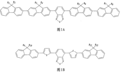
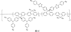
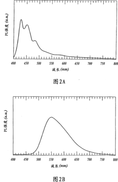
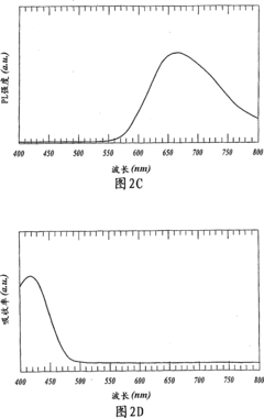
- Green-emitting and red-emitting compounds are dispersed in a blue-emitting matrix in the emission layer, and energy is transferred through the overlap of the emission spectrum of the matrix material and the absorption spectrum of the compound, thereby realizing the transfer from the matrix to the first compound and then to the second compound. Cascade energy transfer of compounds, producing essentially pure white light.
Materials Science Advancements for WOLED Applications
Recent advancements in materials science have significantly contributed to the evolution of White Organic Light-Emitting Diodes (WOLEDs) technology. The development of novel host materials with balanced charge transport properties has been crucial for optimizing electron-hole balance, directly impacting power efficiency. Phosphorescent materials with high quantum yields, particularly iridium and platinum complexes, have enabled more efficient energy transfer mechanisms within the emissive layer.
The emergence of thermally activated delayed fluorescence (TADF) materials represents a breakthrough in WOLED development, allowing for the harvesting of both singlet and triplet excitons without requiring expensive heavy metal complexes. These materials have demonstrated external quantum efficiencies exceeding 20% while maintaining good operational stability, addressing previous limitations in blue TADF emitters.
Charge transport materials have undergone substantial refinement, with new electron transport materials (ETMs) and hole transport materials (HTMs) specifically engineered to create optimal energy level alignment within device structures. The introduction of bipolar host materials capable of transporting both electrons and holes has simplified device architecture while improving charge balance at the recombination zone.
Interface engineering has emerged as a critical focus area, with the development of specialized interlayers that prevent exciton quenching and reduce energy barriers between adjacent functional layers. Composite materials combining multiple functionalities have enabled more streamlined device structures while maintaining excellent charge balance characteristics.
Nanomaterials integration represents another frontier, with quantum dots and nanoparticles being incorporated into WOLED structures to tune emission properties and enhance stability. These materials offer precise control over the emission spectrum and can be engineered to facilitate better charge injection and transport throughout the device.
Computational materials science has accelerated development through predictive modeling of molecular structures and their optoelectronic properties. Machine learning approaches have enabled researchers to identify promising candidate materials with optimal HOMO-LUMO energy levels and charge mobility characteristics without exhaustive experimental screening.
Stability enhancement remains a key research direction, with the development of materials that resist degradation mechanisms such as exciton-polaron quenching and chemical decomposition. Encapsulation technologies and intrinsically stable molecular designs have extended device lifetimes significantly, addressing one of the primary barriers to widespread WOLED adoption in high-brightness applications.
Environmental Impact and Sustainability of WOLED Technologies
The environmental impact of White Organic Light-Emitting Diode (WOLED) technologies extends far beyond their energy consumption metrics. When optimizing electron-hole balance for power efficiency, significant sustainability benefits emerge across the entire lifecycle of these devices. The reduced power consumption directly translates to lower carbon emissions during operation, particularly important as lighting accounts for approximately 15% of global electricity consumption.
Manufacturing processes for WOLEDs with optimized charge carrier balance typically require fewer rare earth elements and heavy metals compared to conventional lighting technologies. This reduction minimizes environmental degradation associated with mining activities and decreases the potential for toxic waste generation. Furthermore, the improved electron-hole balance extends device lifespan by reducing degradation mechanisms, thereby decreasing electronic waste generation rates.
The materials science advancements driving WOLED optimization have spillover effects in green chemistry. Research into balanced charge transport layers has led to the development of more environmentally benign organic semiconductors and processing techniques that utilize fewer harmful solvents. Water-based processing methods are increasingly viable for certain WOLED components, further reducing the environmental footprint of manufacturing.
Supply chain considerations reveal additional sustainability dimensions. Optimized WOLEDs require smaller quantities of critical materials, reducing dependence on geopolitically sensitive resources. The lightweight nature of these devices also decreases transportation-related emissions throughout the distribution network. As manufacturing scales up, these benefits compound significantly across global markets.
End-of-life management presents both challenges and opportunities. While optimized WOLEDs contain fewer hazardous substances than traditional lighting, recycling infrastructure for organic electronics remains underdeveloped. However, the modular design approaches emerging from electron-hole balance research facilitate easier disassembly and material recovery, potentially creating circular economy opportunities.
Policy frameworks increasingly recognize these environmental benefits. Several jurisdictions have implemented energy efficiency standards that indirectly promote optimized WOLED technologies. Carbon pricing mechanisms further enhance the economic case for these devices by monetizing their reduced emissions profile. As sustainability metrics become more integrated into procurement decisions, the market advantage of environmentally superior WOLED technologies continues to strengthen.
Unlock deeper insights with Patsnap Eureka Quick Research — get a full tech report to explore trends and direct your research. Try now!
Generate Your Research Report Instantly with AI Agent
Supercharge your innovation with Patsnap Eureka AI Agent Platform!