

Evaluate WOLED Bias Dependency for Uniform Emission
SEP 16, 20259 MIN READ
Generate Your Research Report Instantly with AI Agent
Patsnap Eureka helps you evaluate technical feasibility & market potential.
WOLED Technology Background and Objectives
White Organic Light-Emitting Diodes (WOLEDs) have emerged as a pivotal technology in the display and lighting industries over the past two decades. Since their initial development in the late 1990s, WOLEDs have evolved from laboratory curiosities to commercial products, offering advantages such as high energy efficiency, excellent color rendering, and form factor flexibility. The technology leverages the electroluminescent properties of organic materials to generate white light through the combination of multiple emissive layers or dopants that produce complementary colors.
The evolution of WOLED technology has been marked by significant improvements in efficiency, lifetime, and color quality. Early WOLEDs suffered from low luminous efficacy and rapid degradation, limiting their practical applications. However, breakthroughs in material science, device architecture, and manufacturing processes have progressively addressed these limitations, enabling WOLEDs to compete with and sometimes surpass traditional lighting technologies in specific applications.
A persistent challenge in WOLED technology is achieving uniform emission across different operating conditions. Particularly problematic is the bias dependency phenomenon, where the spectral output and color coordinates of WOLEDs shift as a function of applied voltage or current density. This effect compromises color stability and can result in inconsistent visual performance, especially in applications requiring precise color reproduction or extended operation across varying brightness levels.
The bias dependency issue stems from complex interactions between charge carriers and different emissive materials within the WOLED structure. As the applied bias changes, the recombination zones within the device can shift, altering the relative contributions of different emitters to the overall spectrum. Additionally, differential aging of various emissive components can exacerbate this effect over the device lifetime.
The primary technical objective of this investigation is to comprehensively evaluate the bias dependency characteristics of state-of-the-art WOLED architectures and identify strategies for minimizing emission variations across operating conditions. This includes quantifying spectral shifts as a function of driving parameters, understanding the underlying physical mechanisms, and exploring novel device structures or materials that could mitigate these effects.
The long-term goal is to develop WOLED technologies that maintain consistent chromaticity coordinates and spectral power distribution regardless of brightness level or operating time. Such advancements would significantly enhance the applicability of WOLEDs in premium display applications, professional lighting, and other fields where color accuracy and stability are paramount. Additionally, understanding and controlling bias dependency could lead to more predictable device aging characteristics, potentially extending the effective lifetime of WOLED products.
Market Analysis for WOLED Display Applications
The WOLED (White Organic Light-Emitting Diode) display market has experienced significant growth in recent years, driven by increasing demand for high-quality displays in premium televisions, smartphones, and other consumer electronics. The global OLED display market was valued at approximately $38.4 billion in 2022 and is projected to reach $72.8 billion by 2026, with WOLEDs representing a substantial segment of this growth trajectory.
Consumer electronics remains the dominant application sector for WOLED displays, accounting for roughly 65% of the total market share. Within this sector, television manufacturers have embraced WOLED technology for their premium product lines, with LG Display leading production capacity. The automotive industry has emerged as the fastest-growing application segment, with a compound annual growth rate exceeding 25% as luxury vehicle manufacturers increasingly incorporate WOLED displays in dashboard systems and entertainment consoles.
Regional analysis indicates that Asia-Pacific dominates the WOLED manufacturing landscape, with South Korea and Japan hosting the majority of production facilities. However, China is rapidly expanding its manufacturing capabilities through substantial investments in OLED technology. North America and Europe represent the largest consumer markets, particularly for high-end WOLED television displays.
The bias dependency issue in WOLED emission uniformity directly impacts market dynamics, as manufacturers must balance production costs against display quality. Industry research indicates that consumers are willing to pay a 15-20% premium for displays with superior uniformity and color accuracy, making the resolution of bias dependency issues economically significant for manufacturers.
Market segmentation analysis reveals that professional markets, including medical imaging, professional video editing, and scientific visualization, have particularly stringent requirements for emission uniformity. These sectors represent smaller volume but higher margin opportunities, with professionals willing to pay substantial premiums for displays that maintain consistent performance across varying brightness levels and viewing conditions.
Competitive analysis shows that manufacturers who have successfully addressed WOLED bias dependency issues command price premiums and enjoy stronger brand loyalty. Consumer reviews and professional evaluations consistently rank emission uniformity among the top five factors influencing purchasing decisions for premium displays, highlighting the market relevance of this technical challenge.
Future market projections indicate that as WOLED technology continues to mature, manufacturers who can deliver superior emission uniformity while maintaining competitive pricing will likely capture increased market share. The growing adoption of WOLED technology in emerging applications such as augmented reality displays and flexible consumer electronics will further amplify the importance of solving bias dependency challenges.
Current Challenges in WOLED Bias Uniformity
White Organic Light-Emitting Diodes (WOLEDs) face significant challenges in achieving uniform emission across varying bias conditions. The primary issue stems from the differential response of various emissive materials to changes in applied voltage, resulting in color shifts and brightness inconsistencies that compromise display quality and energy efficiency.
At the device architecture level, multi-layer WOLED structures exhibit complex electroluminescent behaviors where charge carrier balance becomes increasingly difficult to maintain across different driving voltages. This imbalance manifests as non-uniform emission profiles, particularly evident in transitions between low and high brightness settings, creating noticeable color temperature variations that detract from visual performance.
Material degradation compounds these uniformity challenges, as different organic emitters age at varying rates depending on their operational bias history. Blue emitters, which typically require higher energy for excitation, show accelerated degradation under high bias conditions compared to red and green counterparts. This differential aging creates progressive color imbalance over the device lifetime, particularly problematic for applications requiring color stability such as professional displays and lighting solutions.
Thermal management presents another critical challenge, as localized heating under high bias conditions creates temperature gradients across the panel. These thermal variations alter the emission characteristics of organic materials non-uniformly, further exacerbating bias-dependent color shifts. Current thermal management solutions prove inadequate for maintaining consistent temperature profiles across large-area displays or high-brightness applications.
Manufacturing inconsistencies introduce additional variability, with layer thickness variations and material distribution non-uniformities amplifying bias dependency effects. Even minor deviations in layer formation can significantly alter charge transport properties, creating zones with different electrical characteristics that respond differently to applied bias.
Compensation algorithms currently employed in display drivers offer only partial solutions, as they typically address panel-level variations rather than pixel-specific bias dependencies. These algorithms struggle to account for the complex interplay between material aging, thermal effects, and intrinsic bias-dependent emission characteristics of different color components.
The interface physics between different functional layers presents yet another challenge, with energy barriers at heterojunctions showing voltage-dependent behavior. This results in non-linear charge injection and transport properties that vary with applied bias, creating emission profiles that change not just in intensity but in spectral distribution as voltage changes.
These challenges collectively create significant barriers to achieving truly uniform WOLED emission across the full range of operational bias conditions, necessitating innovative approaches that address both material properties and device architectures simultaneously.
Existing Bias Compensation Methods for WOLEDs
01 Multi-layer structure for uniform emission
White OLEDs can achieve uniform emission through carefully designed multi-layer structures. These structures typically include multiple organic layers such as hole transport layers, electron transport layers, and emission layers with different dopants. By optimizing the thickness and composition of each layer, the device can achieve balanced charge injection and transport, resulting in uniform white light emission across the entire display area.- Multi-layer structure design for uniform emission: White OLEDs can achieve uniform emission through carefully designed multi-layer structures. These designs typically include multiple organic layers with specific functions such as hole transport, electron transport, and emission layers. By optimizing the thickness and composition of each layer, manufacturers can ensure balanced charge injection and transport, resulting in uniform light emission across the device. This approach helps minimize color variation and brightness inconsistencies across the display surface.
- Color mixing techniques for white light generation: Various color mixing approaches are employed to generate uniform white light in WOLEDs. These include using complementary color emitters (such as blue and yellow), RGB (red, green, blue) emitter combinations, or stacked emissive layers. Advanced techniques involve precise doping of host materials with guest emitters at optimized concentrations to achieve the desired color balance. Proper color mixing ensures consistent color temperature and CRI (Color Rendering Index) across the entire emission area of the WOLED.
- Electrode and current distribution optimization: Uniform current distribution is critical for achieving even emission in WOLEDs. This can be accomplished through optimized electrode designs, including transparent conductive materials with high conductivity and uniform thickness. Some approaches incorporate auxiliary electrode structures, bus line patterns, or grid electrodes to minimize voltage drops across large-area displays. These techniques ensure that current density remains consistent across the entire device, preventing brightness variations and hotspots.
- Tandem WOLED architectures: Tandem or stacked WOLED structures consist of multiple emission units connected in series through charge generation layers. This architecture allows for higher luminance efficiency and extended device lifetime while maintaining emission uniformity. The charge generation layers facilitate efficient charge carrier injection into each emission unit, ensuring balanced recombination and uniform light output. Tandem structures can also help distribute the electrical stress across multiple emission units, improving overall device stability and emission uniformity.
- Optical enhancement structures for emission uniformity: Various optical structures can be incorporated into WOLEDs to improve emission uniformity. These include microlens arrays, light extraction layers, photonic crystals, and scattering materials. Such structures help to reduce optical losses due to waveguiding effects and total internal reflection, while also diffusing the emitted light more evenly across the device surface. Additionally, specialized outcoupling enhancement films can be applied to improve both the efficiency and uniformity of light extraction from the WOLED device.
02 Color temperature control techniques
Various techniques are employed to control the color temperature of WOLEDs for uniform emission. These include using multiple emissive materials with complementary emission spectra, adjusting the concentration of dopants in the emissive layers, and implementing color filters. By precisely controlling these parameters, manufacturers can achieve consistent white light with the desired color temperature and prevent color shifts across different viewing angles.Expand Specific Solutions03 Tandem WOLED structures
Tandem WOLED structures consist of multiple OLED units stacked vertically and connected by charge generation layers. This architecture allows for higher luminance efficiency and more uniform emission by distributing the electrical stress across multiple emissive units. The charge generation layers facilitate the recombination of charges in each emissive unit, ensuring balanced emission from different color components and extending device lifetime while maintaining uniform brightness.Expand Specific Solutions04 Pixel design and arrangement for uniform emission
The design and arrangement of pixels in WOLED displays significantly impact emission uniformity. Techniques include optimizing pixel geometry, implementing micro-cavity structures, and using specialized electrode patterns. Advanced pixel designs can minimize optical interference effects and current density variations, resulting in more uniform light distribution across the display. Some designs also incorporate compensation circuits to adjust for variations in driving transistor characteristics.Expand Specific Solutions05 Novel materials for enhanced emission uniformity
Research on novel materials has led to significant improvements in WOLED emission uniformity. These materials include specially designed host-guest systems, phosphorescent and fluorescent emitters with complementary spectra, and advanced transport materials with balanced charge mobility. Some materials feature reduced concentration quenching effects and improved energy transfer efficiency, allowing for more uniform exciton formation and recombination throughout the emissive layer, resulting in consistent brightness and color across the display.Expand Specific Solutions
Leading WOLED Manufacturers and Research Institutions
The WOLED bias dependency for uniform emission technology landscape is currently in a growth phase, with increasing market adoption driven by demand for high-quality displays. The market is expanding rapidly as WOLED technology becomes critical for next-generation display applications, particularly in premium segments. Leading display manufacturers like BOE Technology, TCL China Star, and AUO are advancing technical solutions for bias-dependent emission uniformity, while research institutions including USC and University of Michigan contribute fundamental innovations. Companies such as Nitto Denko, Seoul Viosys, and Sharp are developing specialized materials and components to address emission uniformity challenges. The technology is approaching maturity with commercial implementations, though optimization for power efficiency and color accuracy remains an active development area.
BOE Technology Group Co., Ltd.
Technical Solution: BOE has developed an advanced WOLED (White Organic Light-Emitting Diode) bias dependency management system that optimizes uniform emission across display panels. Their technology incorporates a multi-layer WOLED structure with precisely controlled doping profiles in each emissive layer to minimize color shift under varying bias conditions. The system employs a proprietary compensation algorithm that dynamically adjusts driving voltages based on real-time monitoring of pixel performance, ensuring consistent luminance across the entire display regardless of content brightness levels. BOE's solution includes specialized thin-film transistor (TFT) backplanes designed specifically to deliver stable current to WOLED pixels, reducing the impact of temperature variations on emission uniformity. Their manufacturing process incorporates in-line testing and calibration to identify and correct bias-dependent emission variations before final assembly, resulting in displays with superior color accuracy and lifetime performance.
Strengths: Superior color consistency across varying brightness levels; integrated compensation algorithms reduce visible aging effects; manufacturing scale allows for cost-effective implementation. Weaknesses: Higher power consumption compared to some competing technologies; complex driving schemes may require more sophisticated control circuitry; potential for increased production costs due to additional calibration requirements.
University of Southern California
Technical Solution: USC researchers have developed a groundbreaking approach to WOLED bias dependency management through advanced materials engineering and device physics optimization. Their solution centers on novel host-dopant systems with minimized field-dependent emission characteristics, achieved through molecular design that reduces dipole moment variations under different electric fields. The team has created a comprehensive device model that accurately predicts emission spectrum shifts as a function of driving voltage, enabling precise pre-compensation in display driving schemes. Their research includes innovative charge transport layers with carefully tuned energy levels that maintain consistent carrier balance across operating voltage ranges. USC's approach incorporates quantum mechanical modeling to optimize molecular orientation within emissive layers, reducing the anisotropic emission effects that can contribute to bias-dependent color shifts. The technology also features specialized electrode treatments that ensure uniform charge injection across the active area, further enhancing emission uniformity under varying bias conditions. This research provides fundamental insights into the mechanisms of bias-dependent emission in WOLEDs and practical pathways for implementation in commercial display technologies.
Strengths: Fundamental scientific approach addresses root causes of bias dependency; applicable across different WOLED architectures; provides theoretical framework for further optimization. Weaknesses: Currently at research stage rather than production-ready; may require specialized materials not yet scaled for mass production; implementation complexity may increase manufacturing costs.
Key Patents in WOLED Bias Control Systems
White organic light emitting diode
PatentInactiveTW200708189A
Innovation
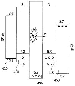
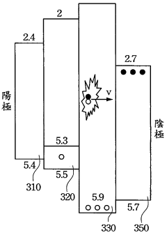
- A symmetrical WOLED structure is introduced with symmetrical light-emitting layers flanking a middle emitting layer, compensating for reduced luminescence in one layer by increasing luminescence in the other, thereby stabilizing light emission across varying voltages.
White organic light-emitting diode
PatentActiveUS7723914B2
Innovation
- A symmetric organic light-emitting device is designed with two symmetric luminescent layers on either side of a central luminescent layer, which maintains luminescent intensity by compensating for decreased intensity in one layer with increased intensity in the other when voltage varies, thereby minimizing color shift.
Material Science Advancements for WOLED Stability
Recent advancements in material science have significantly contributed to enhancing WOLED stability, particularly in addressing bias dependency issues for uniform emission. The development of novel host materials with improved charge transport properties has been a critical breakthrough. These materials feature balanced electron and hole mobility, which reduces charge accumulation at interfaces and minimizes voltage-dependent color shifts across different operating conditions.
Phosphorescent dopant materials have undergone substantial refinement, with new molecular designs incorporating rigid structural elements that resist degradation under electrical stress. These dopants maintain consistent quantum efficiency across varying bias conditions, ensuring color stability throughout the device's operational lifetime. The strategic engineering of dopant concentration gradients within emissive layers has further improved emission uniformity under different driving voltages.
Charge transport layers have been revolutionized through the introduction of crosslinkable materials that form robust interfaces resistant to morphological changes during operation. These materials maintain stable energy levels regardless of applied voltage, preventing shifts in charge injection barriers that typically lead to emission variations. Additionally, the development of graded-energy transport layers has created smoother transitions between functional layers, reducing interfacial voltage drops.
Exciton blocking materials with enhanced thermal and electrochemical stability now effectively confine charge carriers and excitons within the emissive zone regardless of bias conditions. These materials feature wider bandgaps and carefully aligned energy levels that remain effective barriers even under high voltage operation, preventing exciton quenching that would otherwise cause non-uniform emission.
Encapsulation technologies have evolved to incorporate reactive getter materials that actively neutralize degradation agents before they can interact with sensitive emissive materials. Multi-layer barrier films with alternating organic and inorganic components provide superior protection against moisture and oxygen ingress, maintaining material integrity across the device's operational lifetime and reducing bias-dependent degradation pathways.
The integration of these material advances has led to WOLEDs with significantly reduced color point shifts across operating voltages, extended lifetime at high brightness levels, and more consistent luminance efficiency. Current research focuses on developing self-compensating material systems that can dynamically adjust their properties in response to changing electrical conditions, potentially eliminating bias dependency entirely.
Energy Efficiency Considerations in WOLED Bias Design
Energy efficiency represents a critical dimension in WOLED (White Organic Light-Emitting Diode) bias design, directly impacting both device performance and commercial viability. The relationship between bias voltage and emission uniformity creates an inherent trade-off between power consumption and display quality that must be carefully balanced.
When examining WOLED bias dependency, power efficiency emerges as a primary consideration. Higher bias voltages typically generate more uniform emission across the display panel but simultaneously increase power consumption. This relationship becomes particularly significant in battery-powered devices where energy conservation directly affects user experience through device operation time.
Thermal management considerations also play a crucial role in bias design optimization. Higher bias voltages generate additional heat within the WOLED structure, potentially accelerating device degradation and reducing operational lifespan. The thermal load must be carefully managed through bias optimization to prevent hotspots and ensure consistent performance across varying ambient conditions.
Recent advancements in driver circuit design have enabled dynamic bias adjustment techniques that optimize energy consumption based on displayed content. These adaptive systems can modulate bias voltage in real-time, applying higher voltages only when necessary for complex image rendering while reducing power consumption during simpler display tasks. Such intelligent bias management systems have demonstrated energy savings of 15-30% compared to fixed bias implementations.
Material engineering approaches offer another pathway toward improved energy efficiency. Novel emitter materials with lower turn-on voltages can achieve uniform emission at reduced bias levels. Additionally, advanced electrode materials with enhanced charge injection properties minimize resistive losses, further improving overall system efficiency.
The industry has established several metrics for evaluating energy efficiency in WOLED bias design, including power efficiency (measured in lumens per watt), current efficiency (candelas per ampere), and external quantum efficiency (EQE). These standardized measurements enable objective comparison between different bias strategies and their impact on energy consumption while maintaining emission uniformity.
Looking forward, emerging technologies such as machine learning-driven bias optimization algorithms show promise for further efficiency gains. These systems can analyze historical display patterns and environmental conditions to predict optimal bias settings, potentially reducing energy consumption by an additional 10-20% while maintaining or even improving emission uniformity across the display panel.
Unlock deeper insights with Patsnap Eureka Quick Research — get a full tech report to explore trends and direct your research. Try now!
Generate Your Research Report Instantly with AI Agent
Supercharge your innovation with Patsnap Eureka AI Agent Platform!