

Enhance WOLED Anode Modification for Improved Charge Injection
SEP 16, 20259 MIN READ
Generate Your Research Report Instantly with AI Agent
Patsnap Eureka helps you evaluate technical feasibility & market potential.
WOLED Anode Modification Background and Objectives
White Organic Light-Emitting Diodes (WOLEDs) have emerged as a pivotal technology in the display and lighting industries over the past two decades. The evolution of WOLED technology has been characterized by continuous improvements in efficiency, color quality, and operational lifetime. Anode modification represents a critical aspect of this technological progression, as it directly impacts charge injection efficiency—a fundamental parameter determining overall device performance.
The historical development of WOLED anode modification techniques can be traced back to early experiments with indium tin oxide (ITO) surface treatments in the late 1990s. These initial approaches primarily focused on physical and chemical cleaning methods to remove contaminants. As understanding deepened, researchers began exploring more sophisticated modification strategies, including the introduction of buffer layers, work function adjustment through plasma treatments, and the incorporation of self-assembled monolayers (SAMs).
Current technological trends indicate a shift toward multi-layered anode modification architectures that can simultaneously address multiple aspects of charge injection. These include work function alignment, interface dipole formation, and energy level matching between the anode and adjacent organic layers. Additionally, there is growing interest in solution-processable modification materials that can enable cost-effective manufacturing processes.
The primary technical objective of enhancing WOLED anode modification is to optimize hole injection efficiency while maintaining or improving other critical device parameters. Specifically, this entails reducing the energy barrier at the anode-organic interface, minimizing interfacial resistance, and ensuring uniform charge distribution across the active area. These improvements directly translate to lower operational voltages, enhanced power efficiency, and extended device lifetimes.
Secondary objectives include developing modification techniques compatible with flexible substrates to support next-generation flexible display applications, as well as identifying environmentally sustainable materials to replace traditional options containing scarce or toxic elements. Furthermore, there is a pressing need to establish modification methods that maintain performance stability under various environmental conditions, particularly humidity and temperature fluctuations.
The long-term vision for WOLED anode modification extends beyond incremental improvements, aiming for transformative solutions that could enable ultra-high efficiency devices approaching theoretical limits. This includes exploring novel nanomaterials, hybrid organic-inorganic structures, and quantum-engineered interfaces that fundamentally alter charge injection dynamics.
Market Analysis for Enhanced WOLED Technologies
The global WOLED (White Organic Light-Emitting Diode) market continues to experience robust growth, with a market value reaching $38.4 billion in 2022 and projected to expand at a CAGR of 14.7% through 2028. This growth is primarily driven by increasing adoption in high-end displays, lighting applications, and consumer electronics. Enhanced charge injection efficiency through anode modification represents a critical technological advancement that directly addresses market demands for improved device performance and longevity.
Consumer electronics remains the dominant application segment, accounting for approximately 65% of the WOLED market. Within this segment, smartphones and premium televisions are the primary revenue generators, with manufacturers increasingly prioritizing energy efficiency and display quality as key differentiators in competitive markets. The demand for thinner, more flexible displays with higher brightness and lower power consumption continues to drive innovation in anode modification technologies.
The lighting sector represents the fastest-growing application segment for enhanced WOLED technologies, with a growth rate of 18.3% annually. Commercial and residential lighting applications are rapidly adopting WOLED solutions due to their superior energy efficiency, design flexibility, and environmental benefits compared to traditional lighting technologies. Improved charge injection efficiency directly translates to longer device lifetimes and reduced power consumption, addressing key adoption barriers in this sector.
Geographically, East Asia dominates the market with 47% share, led by South Korea, Japan, and China, where major display manufacturers have established production facilities. North America and Europe follow with 24% and 21% market shares respectively, with particular growth in premium consumer electronics and automotive applications. Emerging markets in South Asia and Latin America are showing accelerated adoption rates as manufacturing costs decrease and technology accessibility improves.
The automotive sector represents an emerging high-value application area, with premium vehicle manufacturers incorporating WOLED technology in dashboard displays and interior lighting. This segment values enhanced durability and performance under variable temperature conditions, making improved charge injection particularly relevant. Industry analysts project this segment to grow at 22.5% annually through 2027.
Market research indicates that consumers are willing to pay a premium of 15-20% for devices with improved display quality and battery life, both direct benefits of enhanced charge injection efficiency. This consumer preference is creating strong market pull for technologies that can deliver measurable improvements in these performance metrics, particularly in portable devices where energy efficiency directly impacts user experience.
Current Challenges in WOLED Anode Charge Injection
White Organic Light-Emitting Diodes (WOLEDs) have emerged as a promising technology for next-generation lighting and display applications due to their energy efficiency, flexibility, and color quality. However, the interface between the anode and organic layers presents significant challenges that limit device performance and commercial viability. The primary issue lies in the energy level mismatch between commonly used anode materials (such as indium tin oxide, ITO) and the highest occupied molecular orbital (HOMO) of organic hole transport layers.
This energy barrier results in inefficient hole injection, leading to increased operating voltages, reduced device efficiency, and shortened operational lifetimes. Current ITO anodes typically exhibit work functions around 4.7-4.9 eV, while many organic hole transport materials have HOMO levels deeper than 5.0 eV, creating an inherent injection barrier that impedes charge transport.
Another critical challenge is the surface roughness and chemical inhomogeneity of conventional anode materials. ITO surfaces often contain various defects, contaminants, and non-uniform electrical properties that create localized areas of poor contact with the organic layers. These inconsistencies lead to non-uniform current distribution, increased joule heating, and accelerated device degradation at these interface hotspots.
The stability of the anode-organic interface presents additional complications. Chemical reactions between the anode surface and organic materials can occur during device operation, particularly under elevated temperatures and high current densities. These reactions form interfacial dipoles or trap states that evolve over time, causing progressive increases in driving voltage and decreases in luminance efficiency throughout the device lifetime.
Manufacturing scalability remains problematic for advanced anode modifications. While laboratory-scale techniques like plasma treatment, UV-ozone cleaning, and self-assembled monolayers have shown promise for improving charge injection, these methods often lack consistency in large-scale production environments. The trade-off between process complexity, cost, and performance enhancement has hindered widespread industrial adoption of more sophisticated anode modification techniques.
Environmental concerns further complicate anode development, as traditional ITO contains the scarce and expensive element indium. Alternative materials like graphene, carbon nanotubes, and conductive polymers have been explored, but each presents unique challenges in achieving the optimal combination of transparency, conductivity, and work function required for efficient hole injection in WOLEDs.
The dynamic nature of the anode-organic interface during operation adds another layer of complexity. Under applied bias, charge accumulation, molecular reorientation, and interfacial dipole formation can significantly alter the effective injection barrier. These phenomena are difficult to characterize in situ and vary considerably depending on the specific materials and device architectures employed.
Existing Anode Modification Solutions
01 Anode material modifications for improved charge injection
Various materials can be used to modify the anode in WOLEDs to enhance charge injection efficiency. These modifications include using composite materials, metal oxides, or conductive polymers as anode materials. By optimizing the work function and surface properties of the anode, the energy barrier for hole injection can be reduced, leading to improved device performance and efficiency.- Anode material modifications for improved charge injection: Various materials and modifications can be applied to WOLED anodes to enhance charge injection efficiency. These include using transparent conductive oxides like ITO with specific work functions, incorporating metal dopants, or applying surface treatments to modify the anode's electronic properties. These modifications help reduce energy barriers at the anode-organic interface, leading to more efficient hole injection into the emissive layers of the WOLED device.
- Buffer layer integration between anode and organic layers: Inserting specialized buffer layers between the anode and organic layers can significantly improve charge injection in WOLEDs. These buffer layers, often composed of materials like PEDOT:PSS, metal oxides, or specially designed polymers, help to align energy levels, reduce injection barriers, and prevent unwanted reactions at the interface. The buffer layers can be engineered with specific thickness and composition to optimize hole transport from the anode into the emissive layers.
- Surface treatment techniques for anode modification: Various surface treatment techniques can be applied to modify WOLED anodes for enhanced charge injection. These include plasma treatment, UV-ozone cleaning, chemical functionalization, and physical texturing of the anode surface. Such treatments can alter the work function, increase surface area, remove contaminants, and create favorable dipole moments at the interface, all contributing to improved hole injection efficiency and overall device performance.
- Multilayer anode structures for optimized charge injection: Multilayer anode structures can be designed to optimize charge injection in WOLEDs. These structures typically combine different materials with complementary properties, such as a high-conductivity base layer with a high-work-function top layer. The multilayer approach allows for independent optimization of different anode properties including transparency, conductivity, work function, and surface morphology, resulting in enhanced hole injection and improved device efficiency.
- Doping strategies for enhanced anode performance: Strategic doping of anode materials can significantly enhance charge injection in WOLEDs. Dopants can modify the electronic properties of the anode, particularly its work function and conductivity. Common approaches include metal doping of transparent conductive oxides, incorporation of transition metal compounds, or introduction of p-type dopants at the anode interface. These doping strategies can reduce energy barriers for hole injection and improve overall charge transport in the device.
02 Interface layer engineering between anode and organic layers
Introducing specialized interface layers between the anode and organic layers can significantly improve charge injection in WOLEDs. These buffer layers, such as hole injection layers (HILs) or hole transport layers (HTLs), can be designed with specific electronic properties to facilitate smooth charge transfer from the anode to the emissive layers, reducing operating voltage and enhancing device lifetime.Expand Specific Solutions03 Surface treatment techniques for anode modification
Various surface treatment methods can be applied to modify anode surfaces in WOLEDs, including plasma treatment, UV-ozone cleaning, and chemical functionalization. These treatments can remove contaminants, adjust surface energy, create favorable dipoles, and optimize the work function of the anode, all of which contribute to enhanced charge injection properties and improved device performance.Expand Specific Solutions04 Doping strategies for enhanced anode conductivity
Incorporating dopants into anode materials or adjacent layers can significantly improve charge injection in WOLEDs. Dopants can modify the electronic properties of the anode, increase conductivity, adjust work function, and create additional charge transport pathways. Various dopants including metals, metal salts, and organic compounds can be strategically selected based on their electronic properties to optimize hole injection efficiency.Expand Specific Solutions05 Novel anode architectures for WOLEDs
Innovative anode structures such as multilayer anodes, gradient composition anodes, and patterned anodes can be employed to enhance charge injection in WOLEDs. These architectures can be designed to provide optimal energy level alignment, improved transparency, enhanced conductivity, and better mechanical stability. Advanced fabrication techniques allow for precise control over anode morphology and composition, leading to more efficient and stable devices.Expand Specific Solutions
Leading Companies in WOLED Anode Technology
The WOLED anode modification market is in a growth phase, with increasing demand driven by the expanding OLED display and lighting industries. Major players include Samsung Display and LG Energy Solution, who lead commercial applications, while Novaled GmbH and Idemitsu Kosan have established strong positions in OLED materials development. Research institutions like Korea Electronics Technology Institute and Technical University of Denmark contribute significant innovations. The technology shows varying maturity levels across applications, with companies like Sony and Sumitomo Chemical focusing on enhancing charge injection efficiency through proprietary anode modification techniques. The competitive landscape is characterized by strategic partnerships between material suppliers and device manufacturers to overcome technical challenges in charge transport optimization.
Idemitsu Kosan Co., Ltd.
Technical Solution: Idemitsu Kosan has developed specialized small-molecule organic materials for WOLED anode modification that significantly enhance charge injection efficiency. Their approach centers on engineered hole transport materials with optimized HOMO (Highest Occupied Molecular Orbital) levels that facilitate efficient hole injection from various anode materials. Idemitsu's technology includes gradient-energy hole transport layers where multiple materials with incrementally changing energy levels create a stepwise reduction in injection barriers. They have pioneered thermally stable arylamine derivatives specifically designed for direct contact with anode surfaces, featuring strong adhesion properties and resistance to degradation. Their materials incorporate specialized functional groups that create favorable dipole moments at the anode interface, effectively lowering the energy barrier for hole injection. Additionally, Idemitsu has developed composite hole injection materials that combine the benefits of small molecules and polymers to achieve both excellent charge injection properties and film-forming characteristics.
Strengths: Exceptional thermal stability for extended device lifetimes; materials engineered for compatibility with various anode materials including ITO, metal, and metal oxides; excellent batch-to-batch consistency in material properties. Weaknesses: Vacuum deposition requirements for some materials increase manufacturing complexity; potential for crystallization in certain formulations during extended operation; some specialized materials may have higher production costs.
Novaled GmbH
Technical Solution: Novaled has developed proprietary doping technology for WOLED anode modification that significantly enhances charge injection efficiency. Their approach utilizes p-type dopants to create highly conductive hole transport layers (HTLs) adjacent to the anode, reducing the energy barrier for hole injection. The company's PIN (p-doped, intrinsic, n-doped) OLED architecture incorporates molecular doping technology that creates ultra-low voltage OLEDs with superior power efficiency. Their anode modification techniques include specialized interface layers that improve adhesion between the anode and organic layers while simultaneously enhancing charge injection. Novaled's proprietary dopant materials (NDP series) are specifically designed to optimize the work function alignment between the anode and adjacent organic layers, resulting in devices with lower driving voltages and extended operational lifetimes.
Strengths: Industry-leading doping efficiency resulting in lower operating voltages; proprietary materials portfolio specifically designed for anode interfaces; technology compatible with various anode materials including ITO, metal, and metal oxides. Weaknesses: Higher manufacturing complexity compared to standard approaches; requires precise control of doping concentration; proprietary materials may increase production costs.
Key Patents in Charge Injection Enhancement
Electronic device having an electrode with enhanced injection properties
PatentInactiveUS20060038170A1
Innovation
- The method involves depositing a layer of molecular charge transfer material on an electrode, which is then cross-linked using electron beam irradiation or other processes, enhancing injection properties and thermal stability, and optionally annealing to reduce quenching effects, allowing for improved hole or electron injection in OLEDs.
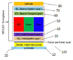
White Organic Light-Emitting Diodes
PatentActiveKR1020190130815A
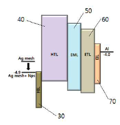
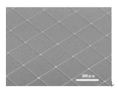
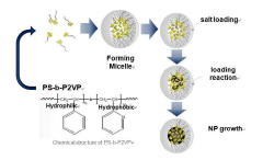
Innovation
- A nanoparticle process using a metal mesh and nanoparticles to form an electrode with a work function similar to ITO, comprising a metal mesh layer, hole injection layer, hole transport layer, light emitting layer, electron transport layer, electron injection layer, and cathode layer on a flexible substrate.
Material Compatibility and Stability Considerations
Material compatibility and stability represent critical considerations in the development of effective WOLED anode modifications for improved charge injection. The interface between the anode material (typically indium tin oxide, ITO) and the organic layers must maintain long-term stability under operational conditions to ensure device longevity. Current research indicates that many modification materials, while enhancing initial charge injection properties, suffer from degradation mechanisms that compromise device performance over time.
Chemical compatibility between the anode modification layer and adjacent organic materials significantly impacts device stability. Modification materials containing reactive functional groups may initiate undesirable side reactions with hole transport materials, leading to the formation of charge traps and subsequent efficiency losses. Studies have shown that materials containing amine groups, while excellent for work function adjustment, can sometimes undergo oxidation at the interface, creating non-radiative recombination centers.
Thermal stability represents another crucial factor, as WOLEDs typically operate at elevated temperatures. Modification materials must maintain their structural integrity and electronic properties across the device's operational temperature range (typically -40°C to 85°C for consumer electronics). Materials with low glass transition temperatures or prone to crystallization under thermal stress can compromise the integrity of the anode-organic interface, leading to delamination and catastrophic device failure.
Environmental stability, particularly resistance to moisture and oxygen penetration, directly influences device lifetime. Many promising anode modification materials demonstrate excellent initial performance but rapidly degrade when exposed to atmospheric conditions during manufacturing or through encapsulation defects. Self-assembled monolayers (SAMs) and transition metal oxides have shown superior stability compared to small-molecule modifiers, though their processing compatibility with existing manufacturing techniques varies significantly.
Processing compatibility must also be considered when selecting anode modification materials. The modification process should not damage previously deposited layers or compromise subsequent deposition steps. Solution-processed modifications must use solvents that do not attack underlying layers, while vacuum-deposited modifications must occur at temperatures compatible with the thermal budget of the entire device stack. Recent advances in atomic layer deposition (ALD) techniques offer promising pathways for creating ultrathin, conformal modification layers with minimal thermal impact.
Long-term electrochemical stability under operational bias represents perhaps the most challenging aspect of anode modification. Materials must withstand continuous charge injection without degradation or migration into adjacent layers. Accelerated lifetime testing protocols have revealed that electrochemical stability often becomes the limiting factor in device longevity, even when other compatibility issues have been addressed.
Environmental Impact of Anode Modification Materials
The environmental implications of anode modification materials in WOLED technology represent a critical consideration in sustainable electronics development. Traditional anode materials and modification layers often contain rare earth elements, heavy metals, and toxic compounds that pose significant environmental challenges throughout their lifecycle. Materials such as molybdenum oxide (MoO3), tungsten oxide (WO3), and transition metal oxides commonly used for anode modification can create environmental burdens during extraction, processing, and disposal phases.
Mining operations for these materials frequently result in habitat destruction, soil degradation, and water pollution. The extraction processes typically consume substantial energy and water resources while generating hazardous waste streams. Additionally, the purification and processing of these materials often involve harsh chemicals and energy-intensive procedures that contribute to carbon emissions and environmental contamination.
During device operation, the environmental impact appears minimal as these materials are effectively encapsulated. However, end-of-life considerations reveal significant challenges. The complex multilayer structure of WOLEDs makes material separation and recovery extremely difficult, resulting in most devices being incinerated or landfilled rather than properly recycled. This leads to potential leaching of toxic compounds into soil and groundwater systems.
Recent research has focused on developing environmentally benign alternatives for anode modification. Bio-based conductive polymers, carbon-based nanomaterials, and solution-processable metal oxides from sustainable sources show promising performance characteristics while reducing environmental footprints. These materials often require lower processing temperatures and fewer toxic solvents during manufacturing.
Life cycle assessment (LCA) studies indicate that transitioning to water-processable anode modification layers could reduce the environmental impact by 30-45% compared to conventional vacuum-deposited metal oxide layers. Furthermore, materials designed with circular economy principles facilitate easier recycling and recovery of valuable components at end-of-life.
Regulatory frameworks worldwide are increasingly addressing the environmental aspects of electronic materials. The European Union's Restriction of Hazardous Substances (RoHS) directive and similar regulations in other regions are driving the industry toward greener alternatives. Companies developing environmentally responsible anode modification technologies may gain competitive advantages as sustainability becomes a market differentiator and compliance requirement.
Future research directions should prioritize biodegradable or easily recyclable anode modification materials that maintain or enhance charge injection properties while minimizing environmental impacts throughout their lifecycle. This approach aligns with broader sustainability goals in the electronics industry and supports the development of truly green display technologies.
Unlock deeper insights with Patsnap Eureka Quick Research — get a full tech report to explore trends and direct your research. Try now!
Generate Your Research Report Instantly with AI Agent
Supercharge your innovation with Patsnap Eureka AI Agent Platform!