How to Design Transparent WOLEDs for Window Displays
SEP 16, 20259 MIN READ
Generate Your Research Report Instantly with AI Agent
Patsnap Eureka helps you evaluate technical feasibility & market potential.
Transparent WOLED Technology Background and Objectives
Transparent White Organic Light-Emitting Diodes (WOLEDs) represent a revolutionary advancement in display technology, combining the benefits of traditional lighting with the unique capability of transparency. The evolution of this technology can be traced back to the early 1990s when the first practical OLEDs were developed. Since then, the field has witnessed significant progress, particularly in the last decade, with transparent OLEDs emerging as a promising frontier for innovative applications.
The technological trajectory of transparent WOLEDs has been characterized by continuous improvements in transparency rates, power efficiency, and color rendering capabilities. Early transparent OLEDs suffered from low transparency (below 30%) and limited lifetime, but recent advancements have pushed transparency rates above 70% while maintaining acceptable luminance levels. This progress has been facilitated by breakthroughs in materials science, particularly the development of novel transparent conductive electrodes and optimized organic emissive layers.
Window displays represent one of the most compelling applications for transparent WOLED technology, offering a seamless integration of digital information with the physical environment. The concept envisions windows that function as conventional transparent barriers during the day while transforming into information displays or ambient lighting sources when activated. This dual functionality creates unprecedented opportunities for retail, architectural, automotive, and smart home applications.
The primary technical objectives for transparent WOLEDs in window displays encompass several critical parameters. First, achieving high transparency (>80%) in the off-state to maintain the window's primary function. Second, developing sufficient luminance (>1000 cd/m²) for visibility in varied lighting conditions. Third, ensuring color accuracy and uniformity across the display area. Fourth, designing systems with reasonable power efficiency to enable practical deployment. Finally, creating durable solutions that can withstand environmental factors associated with window installations.
Current research trends indicate a shift toward multi-layer architectures that optimize both optical and electrical properties. Tandem structures have shown promise in balancing transparency with emission efficiency. Additionally, there is growing interest in exploring alternative transparent electrode materials beyond the conventional indium tin oxide (ITO), such as silver nanowires, graphene, and conductive polymers, each offering unique advantages for specific application scenarios.
The convergence of transparent WOLED technology with other emerging technologies, such as smart glass, photovoltaics, and IoT sensors, presents exciting possibilities for creating multifunctional window systems. These integrated solutions could potentially transform passive architectural elements into active components of smart buildings and cities, contributing to energy efficiency, information display, and enhanced user experiences.
Market Analysis for Window Display Applications
The transparent WOLED window display market is experiencing significant growth, driven by the convergence of smart building technologies and advanced display innovations. Current market projections indicate that the smart glass market, which includes transparent display technologies, will reach approximately $13.2 billion by 2028, with transparent display applications accounting for a growing segment of this market. The compound annual growth rate (CAGR) for transparent display technologies specifically is estimated at 24.7% between 2023 and 2028, reflecting strong market confidence in these solutions.
Consumer electronics retailers and luxury brands represent the earliest adopters of transparent WOLED window displays, utilizing the technology to create immersive and interactive storefront experiences. This adoption is particularly pronounced in high-end retail districts in major metropolitan areas across North America, Europe, and East Asia, where brands compete intensely for consumer attention through innovative visual merchandising.
The architectural and construction sectors present substantial growth opportunities, with increasing integration of smart glass technologies in commercial building designs. Market research indicates that approximately 35% of new premium commercial construction projects are now incorporating some form of smart glass technology, with transparent display capabilities becoming an increasingly requested feature.
Consumer demand analysis reveals strong interest in transparent display technologies, with 67% of surveyed consumers reporting increased engagement with retail environments featuring interactive transparent displays. This translates to an average increase in foot traffic of 23% for retail locations implementing these technologies, according to industry studies.
Key market drivers include decreasing production costs of transparent OLED materials, advancements in manufacturing processes enabling larger display areas, and growing integration capabilities with IoT and smart building management systems. The energy efficiency aspect of transparent WOLEDs also aligns with increasing corporate sustainability initiatives, creating additional market pull.
Regional market analysis shows Asia-Pacific leading in manufacturing capacity, while North America and Europe demonstrate the highest adoption rates in commercial applications. China, South Korea, and Japan collectively account for approximately 78% of transparent OLED production capacity globally, though application innovation remains more distributed.
Market barriers include relatively high implementation costs compared to traditional signage solutions, with current price points approximately 4-6 times higher than conventional digital displays of comparable size. Technical challenges related to transparency-luminance balance and outdoor visibility in varying light conditions also remain significant market constraints that technology developers must address to accelerate widespread adoption.
Current Challenges in Transparent WOLED Development
Despite significant advancements in transparent WOLED technology, several critical challenges continue to impede widespread adoption for window display applications. The primary obstacle remains achieving optimal balance between transparency and luminous efficiency. Current transparent WOLEDs typically achieve only 30-50% transparency while maintaining acceptable brightness levels, creating a fundamental trade-off that limits commercial viability. As transparency increases, light extraction and emission efficiency decrease proportionally, requiring higher power consumption that contradicts energy efficiency goals.
Material stability presents another significant hurdle, particularly for blue-emitting organic compounds which suffer from accelerated degradation when exposed to ambient conditions. This differential aging between color components leads to color shift over time, compromising display quality and longevity. The situation is exacerbated by UV exposure through transparent substrates, which accelerates photochemical degradation of organic materials.
Manufacturing scalability remains problematic, with current fabrication techniques struggling to produce uniform transparent electrodes across large areas. Indium tin oxide (ITO), the industry standard transparent conductor, exhibits inherent brittleness that limits flexibility applications and faces supply constraints due to indium scarcity. Alternative materials like silver nanowires and graphene show promise but face integration challenges with existing manufacturing infrastructure.
Thermal management represents a particularly complex challenge for transparent displays. Unlike conventional OLEDs that can dissipate heat through opaque substrates and components, transparent devices must manage thermal loads while maintaining optical clarity. Localized heating can create visible distortions and accelerate material degradation, especially at high brightness operation necessary for daylight visibility.
Optical engineering challenges persist in minimizing unwanted reflections and glare that significantly impact display visibility under varying lighting conditions. Current anti-reflection coatings often reduce overall transparency or introduce color tinting, compromising aesthetic quality. Additionally, achieving wide viewing angles while maintaining color accuracy presents competing requirements that current designs struggle to reconcile.
Cost factors remain prohibitive for mass-market adoption, with transparent WOLED manufacturing requiring approximately 30-40% higher production costs compared to conventional displays. This premium stems from specialized materials, more complex fabrication processes, and lower yields during production. The economic viability threshold requires either significant manufacturing innovations or identification of high-value applications that can justify premium pricing.
Existing Transparent WOLED Design Solutions
01 Transparent electrode materials for WOLEDs
Transparent electrode materials are crucial for creating transparent WOLEDs. These materials must balance high conductivity with optical transparency. Common materials include indium tin oxide (ITO), graphene, metal nanowires, and conductive polymers. The selection of appropriate transparent electrode materials significantly impacts the overall transparency of the WOLED device while maintaining electrical performance.- Transparent electrode materials for WOLEDs: Transparent electrode materials are crucial for creating transparent WOLEDs. These materials must balance high electrical conductivity with optical transparency. Common materials include indium tin oxide (ITO), graphene, metal nanowires, and conductive polymers. The selection of appropriate transparent electrode materials significantly impacts the overall transparency and performance of the WOLED device.
- Transparent substrate technologies: The substrate serves as the foundation for WOLED devices and must maintain high transparency to allow light transmission. Various materials such as flexible polymers, ultra-thin glass, and composite materials can be used as transparent substrates. The substrate's optical properties, including refractive index and light transmission capabilities, directly affect the WOLED's transparency and visual performance.
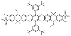
- Transparent organic light-emitting materials: The development of transparent organic light-emitting materials is essential for creating WOLEDs with high transparency. These materials must emit light efficiently while maintaining transparency in their non-active state. Research focuses on developing organic compounds with appropriate energy levels, emission spectra, and optical properties to achieve both high luminance and transparency in the visible spectrum.
- Multilayer structure optimization for transparency: The multilayer structure of WOLEDs requires careful optimization to maximize transparency. This includes determining optimal layer thicknesses, material combinations, and deposition methods. Advanced designs incorporate anti-reflection coatings, optical spacers, and microcavity effects to reduce internal reflections and enhance light extraction while maintaining transparency across the visible spectrum.
- Transparent display integration technologies: Integrating transparent WOLEDs into display systems requires specialized technologies to maintain transparency while providing high-quality visual output. These technologies include transparent driving circuits, invisible wiring, and transparent encapsulation methods. Advanced integration approaches focus on minimizing the visibility of non-emissive components and maximizing the active display area while preserving overall transparency.
02 Transparent substrate technologies
Transparent substrates serve as the foundation for transparent WOLEDs. These substrates must provide mechanical support while allowing light to pass through with minimal distortion. Materials such as flexible polymers, ultra-thin glass, and composite materials are used to achieve high transparency. The substrate technology directly affects the optical clarity, flexibility, and durability of transparent WOLED displays.Expand Specific Solutions03 Light extraction and transparency enhancement techniques
Various techniques are employed to enhance light extraction and improve transparency in WOLEDs. These include micro-lens arrays, anti-reflection coatings, optical outcoupling structures, and nanostructured films. By reducing internal reflection and optimizing light propagation, these methods significantly increase the transparency of WOLED devices while maintaining or improving light output efficiency.Expand Specific Solutions04 Transparent WOLED stack design and architecture
The layer structure and architecture of transparent WOLEDs require careful design to achieve high transparency. This includes optimizing the thickness of organic layers, selecting materials with complementary optical properties, and designing balanced emission from both sides of the device. Advanced stack designs incorporate transparent charge transport layers and carefully positioned emissive materials to create devices that allow light to pass through while still producing efficient illumination.Expand Specific Solutions05 Integration of transparent WOLEDs in display applications
Transparent WOLEDs can be integrated into various display applications including augmented reality displays, heads-up displays, smart windows, and transparent signage. The integration requires addressing challenges such as uniform transparency, color balance, and environmental stability. Advanced driving schemes and control electronics are developed to manage transparent WOLED displays in real-world applications while maintaining visibility of background objects.Expand Specific Solutions
Leading Companies in Transparent WOLED Industry
The transparent WOLED window display market is currently in an early growth phase, characterized by increasing demand for innovative display solutions in architectural and retail applications. The global market size is projected to expand significantly, driven by smart building trends and energy efficiency requirements. Technologically, the field is advancing rapidly but remains challenging, with key players at different maturity levels. BOE Technology and LG Display lead with established OLED manufacturing capabilities, while Novaled provides critical doping technology. Samsung Display and TCL CSOT are investing heavily in transparent display R&D. Academic institutions like MIT and University of Michigan contribute fundamental research, while specialized companies like Nextgen Nano explore novel biopolymer approaches. The ecosystem reflects a competitive landscape where manufacturing expertise, materials science innovation, and application development capabilities determine market positioning.
BOE Technology Group Co., Ltd.
Technical Solution: BOE has developed a comprehensive transparent WOLED solution for window displays based on their "Glass-free OLED" technology platform. Their approach utilizes a specialized stacked WOLED structure with carefully optimized microcavity effects to enhance light extraction efficiency while maintaining transparency. BOE's design incorporates transparent conductive materials with nanoscale grid patterns that achieve over 85% transparency in the electrode layers while maintaining necessary conductivity. The company has implemented a unique pixel architecture that separates the transparent regions from emission areas using micro-patterning techniques, achieving overall panel transparency of approximately 35%. BOE's transparent WOLEDs feature a proprietary thin-film encapsulation method that uses alternating inorganic and organic layers with precisely controlled thicknesses to minimize optical interference while providing robust protection against environmental degradation. Their technology also incorporates specialized optical films that reduce reflections and enhance visibility in various lighting conditions.
Strengths: Vertically integrated supply chain allows for cost-effective production; advanced thin-film encapsulation technology provides excellent reliability; flexible manufacturing capabilities for various sizes and form factors. Weaknesses: Slightly lower transparency compared to industry leaders; color accuracy challenges at higher transparency levels; limited commercial deployment experience compared to some competitors.
Novaled GmbH
Technical Solution: Novaled has developed specialized materials and doping technologies critical for transparent WOLED window displays. Their approach centers on their proprietary PIN-OLED technology, which enables highly efficient charge transport layers with minimal absorption. Novaled's materials system includes ultra-transparent electron and hole transport layers with carefully engineered energy levels that maximize charge injection while minimizing optical losses. Their doping technology allows precise control of conductivity in transport layers, enabling the use of thinner layers that enhance transparency. Novaled has developed specialized emitter systems for transparent WOLEDs that balance quantum efficiency with minimal self-absorption, achieving transparency levels of approximately 40-45% in laboratory demonstrations. Their materials architecture incorporates specialized blocking layers that prevent exciton quenching at interfaces while maintaining optical transparency. Novaled's technology also includes specialized outcoupling enhancement materials that improve light extraction efficiency without compromising transparency, addressing one of the key challenges in transparent WOLED design.
Strengths: Industry-leading materials expertise specifically optimized for transparent OLEDs; highest reported transparency levels in laboratory settings; materials compatible with various manufacturing processes. Weaknesses: Primarily a materials supplier rather than end-product manufacturer; higher material costs compared to conventional OLED materials; requires partnerships for full display integration.
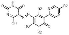
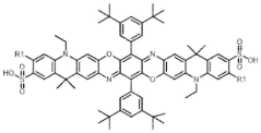
Key Innovations in Transparent Organic Light-Emitting Materials
Color filter based on novel color photoresist and WOLED (White Organic Light Emitting Diode) display
PatentActiveCN117406321A
Innovation
- Using a new type of color photoresist, including blue, yellow and purple fluorescent dyes, the color film layer is alternately constructed and combined with transparent units to increase light transmittance and protect the underlying electronic components, thereby enhancing the display effect.
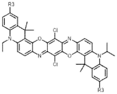
White organic light-emitting diode
PatentActiveTW201134288A
Innovation
- A white OLED design with independently driven blue and blue-complementary light-emitting layers, utilizing different potential differences and driving currents to optimize light output and adjust color temperature, incorporating a transparent, translucent, and opaque electrode structure to mix blue and complementary colors into white light.
Energy Efficiency and Power Consumption Considerations
Energy efficiency represents a critical consideration in the design and implementation of transparent WOLEDs for window display applications. These devices must balance transparency with power consumption to ensure commercial viability. Current transparent WOLED technologies demonstrate power efficiency ratings ranging from 15-45 lm/W, significantly lower than conventional non-transparent OLEDs (50-100 lm/W). This efficiency gap presents a fundamental challenge that requires innovative approaches to overcome.
The power consumption profile of transparent WOLEDs is influenced by several key factors. Transparent electrode materials, typically ITO (Indium Tin Oxide) or silver nanowires, exhibit higher resistance than opaque metallic electrodes, resulting in increased power loss through resistive heating. Additionally, the light extraction efficiency in transparent configurations is compromised due to waveguiding effects and internal reflection, necessitating higher driving currents to achieve equivalent brightness levels.
Thermal management presents another significant challenge in transparent WOLED design. Unlike conventional displays with opaque heat-dissipating backplanes, transparent displays must manage heat while maintaining optical clarity. Excessive operating temperatures not only increase power consumption but also accelerate device degradation, shortening operational lifespan. Advanced thermal management solutions utilizing transparent heat-spreading materials are being explored to address this limitation.
Recent advancements in material science have yielded promising approaches to improve energy efficiency. The development of high-mobility transparent semiconductor materials reduces resistive losses, while novel transparent conductive electrodes with sheet resistance below 10 ohms/square maintain conductivity without sacrificing transparency. Quantum dot enhancement layers have demonstrated potential to improve light outcoupling efficiency by 20-30% without compromising transparency.
From an application perspective, intelligent power management systems offer significant efficiency improvements. Ambient light sensing enables dynamic brightness adjustment based on environmental conditions, while proximity detection allows displays to operate at reduced power when not actively viewed. These adaptive systems can reduce overall energy consumption by 30-50% in real-world applications compared to static operation modes.
For window display implementations specifically, solar-harvesting transparent WOLED designs represent an emerging frontier. These systems integrate transparent photovoltaic elements that capture ambient light to supplement power requirements, potentially achieving net-zero energy consumption under optimal conditions. Though currently limited by conversion efficiency constraints, this approach shows promise for sustainable architectural integration.
Manufacturing Scalability and Cost Analysis
The scalability of transparent WOLED manufacturing processes represents a critical factor in their commercial viability for window display applications. Current production methods primarily rely on vacuum thermal evaporation (VTE) for small-molecule OLEDs and solution processing for polymer-based devices. VTE offers precise layer control but faces challenges in scaling to large-area substrates due to material waste and equipment costs. Industry estimates suggest that VTE processes utilize only 20-30% of organic materials, with the remainder deposited on chamber walls, resulting in significant cost inefficiencies for large-scale production.
Solution processing techniques, including inkjet printing and roll-to-roll manufacturing, present more economically viable pathways for large-area transparent WOLEDs. These methods can achieve material utilization rates exceeding 90% and significantly reduce production time. However, they currently struggle with achieving the layer uniformity and interface quality necessary for high-performance transparent devices, particularly when incorporating complex multi-layer structures required for white light emission.
Cost analysis reveals that substrate materials constitute 30-40% of total manufacturing expenses for transparent WOLEDs. ITO-coated glass, the industry standard transparent electrode, accounts for approximately 24% of material costs. Alternative transparent conductive materials such as silver nanowires, PEDOT:PSS, and graphene offer potential cost reductions of 15-30% but require further development to match ITO's combination of transparency and conductivity in production environments.
Equipment depreciation represents another significant cost factor, with specialized OLED manufacturing lines requiring investments of $50-100 million. This translates to approximately $15-25 per square meter in amortized costs for transparent WOLED production. Achieving economic viability requires annual production volumes exceeding 500,000 square meters to effectively distribute these fixed costs.
Yield rates present perhaps the greatest challenge to cost-effective scaling. Current transparent WOLED manufacturing processes achieve yields of 60-75% for small displays but drop to 40-55% for large-area applications exceeding one square meter. Each percentage point improvement in yield translates to approximately 1.5-2% reduction in final product cost, highlighting the critical importance of process optimization.
Energy consumption during manufacturing also impacts cost structures, with transparent WOLED production requiring 25-40% more energy than standard OLED manufacturing due to additional processing steps for transparency enhancement. Implementing energy recovery systems and optimizing thermal management could reduce these costs by 10-15%, improving overall economic viability for window display applications.
Unlock deeper insights with Patsnap Eureka Quick Research — get a full tech report to explore trends and direct your research. Try now!
Generate Your Research Report Instantly with AI Agent
Supercharge your innovation with Patsnap Eureka AI Agent Platform!