

Improving WOLED Yield in Mass Production Environments
SEP 15, 20259 MIN READ
Generate Your Research Report Instantly with AI Agent
PatSnap Eureka helps you evaluate technical feasibility & market potential.
WOLED Technology Evolution and Production Objectives
White Organic Light-Emitting Diode (WOLED) technology has evolved significantly since its inception in the early 1990s. The journey began with the pioneering work of researchers at Eastman Kodak who developed the first practical OLED devices. Initially, these devices suffered from poor efficiency, limited lifetime, and manufacturing challenges that restricted their commercial viability. The evolution of WOLED technology has been marked by continuous improvements in materials science, device architecture, and manufacturing processes.
By the early 2000s, the introduction of phosphorescent emitters represented a significant breakthrough, dramatically improving energy efficiency. This was followed by the development of tandem structures and the implementation of microcavity effects to enhance light extraction. The past decade has witnessed remarkable advancements in WOLED technology, particularly in the areas of blue emitter stability, thin-film encapsulation techniques, and the integration of color filters for improved color gamut.
Current WOLED production objectives primarily focus on yield improvement in mass production environments. Yield rates directly impact manufacturing costs and ultimately determine market competitiveness. Industry benchmarks suggest that achieving yield rates above 85% is essential for sustainable profitability in the display industry. However, many manufacturers still struggle with yield rates between 60-75% for complex WOLED panels, particularly in larger formats and higher resolutions.
Key production objectives include reducing pixel defects caused by particle contamination, improving the uniformity of organic layer deposition, enhancing the reliability of thin-film encapsulation, and optimizing the alignment precision in color filter processes. Additionally, manufacturers aim to develop more robust testing and quality control protocols that can identify potential failures earlier in the production process.
The technological roadmap for WOLED yield improvement encompasses several parallel tracks. Short-term objectives (1-2 years) focus on optimizing existing processes through statistical process control and incremental equipment modifications. Medium-term goals (3-5 years) involve the implementation of next-generation deposition technologies and automated optical inspection systems. Long-term objectives (5+ years) include the development of revolutionary manufacturing approaches such as solution-processed OLEDs and roll-to-roll production techniques.
Achieving these objectives requires a multidisciplinary approach combining advances in materials science, precision engineering, and computational modeling. Success will be measured not only by improved yield rates but also by the ability to maintain these improvements while scaling to larger substrate sizes and implementing more complex device architectures.
Market Analysis for High-Yield WOLED Products
The WOLED (White Organic Light-Emitting Diode) market has experienced significant growth in recent years, driven by increasing demand for high-quality display technologies across multiple industries. Current market projections indicate that the global OLED market is expected to reach $48.8 billion by 2026, with WOLEDs representing a substantial segment of this market due to their superior color reproduction and energy efficiency compared to traditional display technologies.
Consumer electronics remains the primary application sector for high-yield WOLED products, with smartphones and premium televisions leading adoption. The television segment has shown particularly strong growth, with annual increases of 40-50% in WOLED panel shipments as manufacturers transition their premium lines to this technology. Additionally, automotive displays are emerging as a high-potential growth sector, with luxury vehicle manufacturers increasingly incorporating WOLED technology into dashboard and entertainment systems.
Market analysis reveals that yield rates significantly impact pricing structures and market penetration. Current industry average yield rates for WOLED production hover between 60-70%, with top manufacturers achieving up to 85% in optimized production environments. Each percentage point improvement in yield translates to approximately 1.2-1.5% reduction in production costs, creating substantial competitive advantages for manufacturers who can consistently achieve higher yields.
Regional market distribution shows Asia-Pacific dominating WOLED manufacturing, with South Korea and China accounting for over 75% of global production capacity. However, European and North American markets represent the highest revenue potential for premium high-yield WOLED products, particularly in specialized applications such as medical displays and professional creative monitors where quality consistency is paramount.
Consumer preference analysis indicates growing awareness and demand for higher quality displays, with 68% of premium device purchasers citing display quality as a "very important" factor in purchasing decisions. This trend supports the market case for investing in yield improvement technologies, as the resulting quality consistency directly addresses consumer expectations.
The competitive landscape features intense rivalry among major display manufacturers, with companies investing heavily in proprietary yield improvement technologies as a key differentiator. Market leaders have demonstrated that achieving consistently higher yields not only reduces costs but also enables them to secure premium pricing through quality guarantees and reduced defect rates, resulting in profit margin improvements of 3-5% compared to industry averages.
Forecast models predict that manufacturers achieving breakthrough improvements in WOLED yield rates could capture up to 15% additional market share within their target segments over a 3-year period, highlighting the strategic importance of yield optimization as both a cost reduction and market expansion strategy.
Current WOLED Manufacturing Challenges
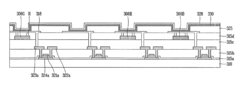
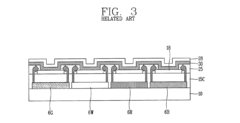
Despite significant advancements in WOLED (White Organic Light-Emitting Diode) technology, mass production environments continue to face substantial manufacturing challenges that directly impact yield rates. The complex multi-layer structure of WOLED panels, which typically incorporates red, green, blue, and sometimes yellow emitting materials, creates numerous opportunities for defects during the production process.
Material degradation represents a primary challenge, particularly for blue emitters which exhibit shorter lifespans compared to their red and green counterparts. This inconsistent degradation leads to color shifting over time, affecting both production consistency and long-term device performance. The industry continues to search for more stable blue phosphorescent materials that can match the efficiency and longevity of other emitters.
Contamination control remains exceptionally difficult in WOLED manufacturing. Even microscopic particles or moisture can cause catastrophic device failure, necessitating extensive cleanroom protocols. Current production lines struggle to maintain the required parts-per-billion cleanliness levels consistently across high-volume operations, resulting in significant yield losses.
Layer uniformity presents another critical challenge. The precision required for depositing multiple organic layers, each only nanometers thick, stretches the capabilities of existing vapor deposition equipment. Variations in layer thickness as small as ±2nm can cause visible defects and color inconsistencies across the panel surface, particularly problematic for larger display formats.
Encapsulation technology limitations further compound yield issues. Current barrier films and encapsulation methods cannot completely prevent oxygen and moisture ingress over extended periods, leading to dark spots and edge degradation. This becomes especially problematic as manufacturers push toward thinner, more flexible display designs.
Electrical defects, including short circuits and pixel failures, occur frequently during the integration of the OLED stack with the thin-film transistor (TFT) backplane. The industry standard acceptable defect rate remains significantly higher than for LCD technology, with "dead pixels" continuing to be a major yield detractor.
Scaling challenges persist as manufacturers attempt to transfer laboratory-proven processes to mass production environments. Techniques that produce excellent results in small-scale research settings often encounter unforeseen complications when implemented on production lines handling substrates measuring several square meters.
Testing and quality control methodologies struggle to keep pace with production speeds. Current inspection systems cannot detect all potential failure modes in real-time, meaning some defects are only discovered after significant material and processing investments, substantially increasing the cost of low yields.
Current Yield Improvement Methodologies
01 Optimization of WOLED layer structure
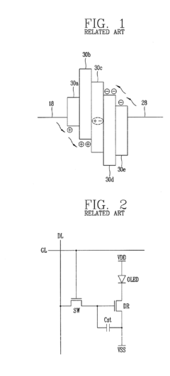
The yield of White Organic Light-Emitting Diodes can be improved by optimizing the layer structure. This includes designing multi-layer structures with precisely controlled thicknesses, implementing tandem structures, and using intermediate connecting layers. These structural optimizations help to balance charge transport, enhance light extraction efficiency, and improve device stability, all contributing to higher manufacturing yields and better performance.- Optimization of WOLED device structure for improved yield: Various structural optimizations can enhance WOLED manufacturing yield. These include optimizing layer thicknesses, employing multi-unit stacked architectures, and using specialized electrode configurations. Proper alignment of emission layers and strategic placement of charge transport layers can reduce defects and improve uniformity. These structural modifications help balance charge distribution and enhance light extraction efficiency, resulting in higher production yields and more consistent device performance.
- Advanced materials selection for high-yield WOLED production: Selection of appropriate organic materials significantly impacts WOLED manufacturing yield. Using high-purity host materials, stable phosphorescent dopants, and robust charge transport materials reduces degradation and defect formation. Novel materials with improved thermal stability and resistance to operational stress extend device lifetime and manufacturing consistency. Careful material selection and compatibility testing between adjacent layers minimizes interfacial defects that commonly reduce production yields.
- Process control techniques for WOLED yield enhancement: Precise process control during WOLED manufacturing significantly improves yield rates. Implementing strict environmental controls during deposition, optimizing vacuum levels, and maintaining consistent deposition rates reduce variability. Advanced monitoring systems for temperature, pressure, and contamination levels help identify and correct process deviations before they impact yield. Statistical process control methods and real-time feedback systems enable continuous optimization of manufacturing parameters to maximize production efficiency.
- Color tuning methods for consistent WOLED performance: Achieving consistent color performance across production batches is crucial for high WOLED yields. Methods include precise dopant concentration control, multi-emissive layer designs with complementary emission spectra, and tandem structures with separate blue, green, and red emission units. Advanced color calibration techniques during manufacturing help identify and correct color variations early in the production process. These approaches ensure uniform color temperature and CRI values across manufactured devices, reducing rejection rates.
- Testing and quality control systems for WOLED production: Comprehensive testing and quality control systems are essential for identifying defects and improving WOLED yields. Automated optical inspection systems detect pixel defects, non-uniformities, and color variations. Electrical testing protocols identify short circuits, open circuits, and abnormal I-V characteristics. Accelerated lifetime testing helps predict long-term reliability issues. Implementation of machine learning algorithms for defect pattern recognition enables continuous yield improvement through predictive maintenance and process refinement.
02 Material selection and composition for emission layers
Careful selection of organic materials for emission layers significantly impacts WOLED yield. Using combinations of red, green, and blue emitters with optimized ratios helps achieve balanced white light emission. Phosphorescent materials, quantum dots, and specially designed host-dopant systems can enhance quantum efficiency. Advanced material purification techniques and composition control during manufacturing contribute to consistent device performance and higher production yields.Expand Specific Solutions03 Manufacturing process improvements
Enhanced manufacturing processes directly improve WOLED yield. Techniques such as vacuum thermal evaporation with precise deposition control, solution processing methods like inkjet printing, and advanced patterning technologies reduce defects and increase consistency. Implementing clean room environments, optimized annealing processes, and improved encapsulation techniques protect devices from contamination and degradation, resulting in higher production yields.Expand Specific Solutions04 Electrode and interface engineering
Engineering of electrodes and interfaces between layers is crucial for WOLED yield improvement. Implementing work function matching between electrodes and organic layers enhances charge injection. Buffer layers and interface modification techniques reduce energy barriers and prevent exciton quenching. Transparent conductive materials with high conductivity and transparency optimize light extraction, while specialized surface treatments improve adhesion between layers and reduce defects.Expand Specific Solutions05 Device architecture and pixel design
Advanced device architectures and pixel designs contribute to higher WOLED yields. Implementing microcavity structures enhances color purity and efficiency. Top-emission designs improve light extraction compared to bottom-emission configurations. Pixel layout optimization reduces current crowding and heat generation. Specialized color filter arrangements and light management structures maximize efficiency, while redundancy features in pixel design improve manufacturing tolerance and yield.Expand Specific Solutions
Key WOLED Industry Players and Competition
The WOLED yield improvement landscape is currently in a mature growth phase, with significant market expansion driven by increasing demand for high-quality displays. The global market size is projected to grow substantially as WOLED technology becomes more prevalent in premium display applications. From a technical maturity perspective, industry leaders like Samsung Electronics, BOE Technology, and TCL China Star Optoelectronics have established advanced manufacturing processes, while companies such as Applied Materials, KLA Corp, and ASML Holding provide critical equipment solutions for yield optimization. Taiwan Semiconductor and Micron Technology contribute expertise in semiconductor integration, while research partnerships with institutions like University of Southern California and University of Michigan are advancing next-generation WOLED fabrication techniques. The competitive landscape shows a balance between established display manufacturers and specialized equipment providers working to overcome mass production challenges.
BOE Technology Group Co., Ltd.
Technical Solution: BOE has developed an advanced evaporation process control system specifically for WOLED production that utilizes real-time monitoring and AI-driven adjustments. Their solution incorporates multi-zone temperature control during organic material deposition, maintaining temperature variations within ±0.5°C across large substrates. The system employs in-situ optical monitoring to detect thickness variations during evaporation, with feedback algorithms that dynamically adjust deposition rates. BOE's approach also includes specialized shadow masks with tension compensation mechanisms that reduce pattern distortion by up to 40% compared to conventional masks, significantly improving pixel alignment accuracy in mass production environments.
Strengths: Exceptional precision in large-panel manufacturing with industry-leading temperature control; integrated AI systems that continuously optimize parameters based on production data. Weaknesses: Higher initial implementation costs compared to traditional systems; requires specialized training for operators to fully utilize the advanced monitoring capabilities.
Samsung Electronics Co., Ltd.
Technical Solution: Samsung has pioneered a comprehensive WOLED yield improvement system combining material purification techniques and advanced encapsulation technology. Their solution features a proprietary multi-stage organic material purification process that achieves 99.99% purity levels, significantly reducing defects caused by contaminants. The system incorporates hybrid deposition techniques that optimize both small molecule and polymer materials in different WOLED layers. Samsung's thin-film encapsulation (TFE) technology employs alternating inorganic and organic layers with precise thickness control, reducing moisture penetration rates to less than 10^-6 g/m²/day. Their manufacturing execution system (MES) integrates defect detection algorithms that can identify pattern anomalies as small as 3μm, enabling real-time process corrections.
Strengths: Vertical integration allowing control over the entire manufacturing process from materials to finished displays; sophisticated defect prediction models based on extensive production data. Weaknesses: Complex implementation requiring significant capital investment; some proprietary materials have limited availability and higher costs than industry-standard alternatives.
Critical Patents in WOLED Manufacturing
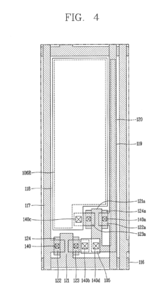
White Organic Light Emitting Diode Display Device and Method of Fabricating the Same
PatentActiveUS20120161141A1
Innovation
- A W-OLED display device with a passivation layer made of silicon nitride, featuring holes to expose and remove outgassing from color filters, and a thickness of 1000-5000 Å to prevent wave guiding, along with a method involving curing processes to remove outgases effectively.
White organic light-emitting diode
PatentActiveUS7723914B2
Innovation
- A symmetric organic light-emitting device is designed with two symmetric luminescent layers on either side of a central luminescent layer, which maintains luminescent intensity by compensating for decreased intensity in one layer with increased intensity in the other when voltage varies, thereby minimizing color shift.
Material Science Advancements for WOLED Production
Recent advancements in material science have significantly contributed to improving WOLED (White Organic Light-Emitting Diode) yield in mass production environments. The development of novel host materials with enhanced thermal stability has addressed one of the primary challenges in WOLED manufacturing - the degradation of organic materials during high-temperature deposition processes. These new materials demonstrate glass transition temperatures exceeding 150°C, substantially reducing molecular decomposition during fabrication.
Phosphorescent dopant innovations have revolutionized WOLED efficiency and stability. Third-generation iridium-based complexes now achieve nearly 100% internal quantum efficiency while maintaining color purity across extended operational lifetimes. These materials exhibit reduced concentration quenching effects, allowing for more consistent emission characteristics even with minor concentration variations during manufacturing.
Electron transport layer (ETL) materials have undergone significant refinement, with new compounds featuring improved electron mobility and reduced sensitivity to moisture. The introduction of phosphine oxide-based ETLs has demonstrated superior resistance to degradation during encapsulation processes, directly contributing to higher production yields by minimizing post-deposition failures.
Barrier and encapsulation materials represent another critical advancement area. Atomic Layer Deposition (ALD) techniques now enable the creation of ultra-thin (< 10nm) barrier films with water vapor transmission rates below 10^-6 g/m²/day. These advanced barriers effectively protect sensitive organic materials from environmental contaminants while maintaining flexibility for next-generation display applications.
Solution-processable materials are emerging as game-changers for high-volume WOLED production. Recent developments in water/alcohol-soluble hole injection materials eliminate the need for vacuum deposition of certain layers, reducing manufacturing complexity and associated yield losses. These materials demonstrate comparable device performance to their vacuum-deposited counterparts while offering significant advantages in processing uniformity across large substrates.
Cross-linkable interface materials represent another promising direction, allowing for the creation of robust interlayer boundaries that resist intermixing during sequential layer deposition. These materials can be selectively polymerized after deposition, creating stable interfaces that maintain distinct functional layer separation even under challenging manufacturing conditions, thereby enhancing overall device yield and performance consistency.
Environmental Impact of WOLED Manufacturing Processes
The manufacturing processes of White Organic Light-Emitting Diodes (WOLEDs) involve several environmentally sensitive components and procedures that warrant careful consideration. Traditional WOLED production relies heavily on rare earth metals, organic solvents, and energy-intensive vacuum deposition techniques, all of which contribute to significant environmental footprints.
Chemical waste management represents one of the most pressing environmental challenges in WOLED manufacturing. The organic materials used in the emissive layers often require halogenated solvents for processing, which can lead to hazardous waste streams if not properly managed. Industry data suggests that for every square meter of WOLED panel produced, approximately 0.5-1.2 liters of chemical waste is generated, necessitating specialized treatment facilities.
Energy consumption during manufacturing constitutes another major environmental concern. Vacuum thermal evaporation (VTE), the predominant deposition method for WOLED materials, operates at high temperatures and requires substantial power input. Recent studies indicate that energy requirements for WOLED production range from 230-280 kWh per square meter of display area, significantly higher than LCD manufacturing at 180-220 kWh per square meter.
Water usage in WOLED fabrication processes, particularly for cleaning and cooling operations, presents additional environmental challenges. A typical WOLED production facility consumes between 5-7 gallons of ultra-pure water per square foot of panel area, with much of this water requiring treatment before discharge due to contamination with trace metals and organic compounds.
Emissions of volatile organic compounds (VOCs) during manufacturing pose both environmental and health risks. Without proper abatement systems, WOLED production can release 0.8-1.5 kg of VOCs per 1,000 square meters of panel area. These emissions contribute to photochemical smog formation and may have adverse health effects on workers and surrounding communities.
Recent technological innovations are addressing these environmental concerns through several approaches. Solution-based processing techniques are reducing solvent requirements by 40-60% compared to traditional methods. Additionally, closed-loop recycling systems for rare materials like indium and gallium are improving resource efficiency, with recovery rates now reaching 70-85% in advanced facilities.
The industry is also witnessing a transition toward greener manufacturing practices, with leading manufacturers implementing ISO 14001 environmental management systems and pursuing carbon neutrality goals. These efforts, combined with regulatory pressures in key manufacturing regions, are driving continuous improvement in the environmental performance of WOLED production processes.
Unlock deeper insights with PatSnap Eureka Quick Research — get a full tech report to explore trends and direct your research. Try now!
Generate Your Research Report Instantly with AI Agent
Supercharge your innovation with PatSnap Eureka AI Agent Platform!