How to Innovate with Quasicrystal in Transparent Conductors?
Quasicrystal Conductors: Background and Objectives
Quasicrystals, discovered in 1982 by Dan Shechtman, represent a unique class of materials that possess long-range order but lack periodicity. This groundbreaking discovery challenged the conventional understanding of crystalline structures and opened up new avenues for materials science research. In recent years, the potential application of quasicrystals in transparent conductors has garnered significant attention from both academia and industry.
The field of transparent conductors has traditionally been dominated by materials such as indium tin oxide (ITO) and fluorine-doped tin oxide (FTO). However, these materials face limitations in terms of cost, flexibility, and performance. The exploration of quasicrystalline structures in transparent conductors aims to overcome these challenges and push the boundaries of what is possible in optoelectronic devices.
The primary objective of this research is to investigate the potential of quasicrystals to revolutionize transparent conductor technology. By leveraging the unique properties of quasicrystalline structures, researchers aim to develop materials that exhibit superior electrical conductivity while maintaining high optical transparency. This combination of properties is crucial for applications in solar cells, touch screens, smart windows, and other advanced optoelectronic devices.
One of the key advantages of quasicrystals lies in their ability to form complex, aperiodic structures that can potentially enhance electron mobility while minimizing light scattering. This unique structural characteristic offers the possibility of creating transparent conductors with improved performance compared to traditional crystalline materials.
The evolution of quasicrystal research in transparent conductors has been marked by several significant milestones. Initial studies focused on understanding the fundamental properties of quasicrystalline materials and their potential applications in various fields. As the research progressed, scientists began to explore the synthesis and characterization of quasicrystalline thin films suitable for transparent conductor applications.
Recent advancements in nanofabrication techniques and computational modeling have accelerated the development of quasicrystal-based transparent conductors. These tools have enabled researchers to design and optimize quasicrystalline structures with tailored electronic and optical properties, paving the way for practical applications in next-generation devices.
The integration of quasicrystals into transparent conductor technology represents a convergence of fundamental materials science and applied engineering. This interdisciplinary approach aims to address the growing demand for high-performance, cost-effective transparent conductors in various industries, including electronics, energy, and automotive sectors.
As research in this field continues to evolve, the ultimate goal is to develop commercially viable quasicrystal-based transparent conductors that outperform existing technologies. This ambitious objective requires overcoming challenges related to large-scale synthesis, material stability, and integration into existing manufacturing processes.
Market Analysis for Transparent Conductive Materials
The transparent conductive materials market has been experiencing significant growth due to the increasing demand for touchscreens, displays, and photovoltaic devices. Traditional materials like Indium Tin Oxide (ITO) have dominated the market, but rising costs and supply constraints have driven the search for alternatives. This has opened opportunities for innovative materials such as quasicrystal-based transparent conductors.
The global transparent conductive films market is projected to expand substantially in the coming years, driven by the growing adoption of smartphones, tablets, and other electronic devices with touch interfaces. The automotive sector is also emerging as a key market, with increasing integration of touch panels and displays in vehicles. Additionally, the renewable energy sector, particularly solar panels, represents a significant growth area for transparent conductive materials.
Quasicrystal-based transparent conductors offer several potential advantages over traditional materials. They can provide improved conductivity and transparency, along with enhanced durability and flexibility. These properties make them particularly attractive for next-generation flexible electronics and wearable devices. The unique atomic structure of quasicrystals also offers the potential for improved light management, which could be beneficial in solar cell applications.
However, the market for quasicrystal-based transparent conductors is still in its nascent stages. Current market share is minimal compared to established materials like ITO, silver nanowires, and carbon nanotubes. The primary challenges include scaling up production processes and reducing manufacturing costs to compete with existing solutions.
Despite these challenges, the potential market for quasicrystal-based transparent conductors is substantial. As electronic devices continue to evolve towards more flexible and durable form factors, the demand for advanced transparent conductive materials is expected to grow. The automotive industry's shift towards electric vehicles and advanced infotainment systems also presents a significant opportunity.
To capitalize on this potential, companies investing in quasicrystal-based transparent conductors will need to focus on demonstrating clear performance advantages and cost-effectiveness compared to existing solutions. Collaboration with device manufacturers and integration into existing production processes will be crucial for market adoption. As research progresses and manufacturing techniques improve, quasicrystal-based materials could carve out a significant niche in the transparent conductive materials market, particularly in applications requiring high performance and unique properties.
Current Challenges in Quasicrystal Conductor Development
The development of quasicrystal-based transparent conductors faces several significant challenges that hinder their widespread adoption and commercialization. One of the primary obstacles is the difficulty in synthesizing large-scale, high-quality quasicrystalline materials suitable for transparent conductor applications. The unique aperiodic structure of quasicrystals makes their growth process complex and often results in defects and impurities that can negatively impact their electrical and optical properties.
Another major challenge lies in achieving the optimal balance between transparency and conductivity. While quasicrystals offer promising electronic properties due to their unique atomic arrangements, maintaining high optical transparency while simultaneously enhancing electrical conductivity remains a significant hurdle. This balance is crucial for applications in optoelectronic devices, such as solar cells and displays.
The integration of quasicrystal-based transparent conductors into existing manufacturing processes presents another substantial challenge. Current industrial production methods are primarily optimized for periodic crystalline materials, and adapting these processes to accommodate the unique properties of quasicrystals requires significant research and development efforts. This includes developing new deposition techniques, etching processes, and patterning methods that are compatible with quasicrystalline structures.
Stability and durability of quasicrystal conductors under various environmental conditions pose additional challenges. Many potential applications for transparent conductors involve exposure to heat, humidity, and mechanical stress. Ensuring that quasicrystal-based materials maintain their electrical and optical properties over extended periods under these conditions is crucial for their practical implementation.
Furthermore, the cost-effectiveness of quasicrystal conductor production remains a significant barrier. Current synthesis methods for high-quality quasicrystals are often complex and expensive, making it difficult to compete with established transparent conductor technologies such as indium tin oxide (ITO). Developing more economical production techniques while maintaining material quality is essential for the commercial viability of quasicrystal-based transparent conductors.
Lastly, there is a need for more comprehensive understanding of the fundamental physics governing the electronic and optical properties of quasicrystals. While significant progress has been made in theoretical modeling and experimental characterization, many aspects of quasicrystal behavior in the context of transparent conductors remain poorly understood. This knowledge gap hampers the development of optimized materials and devices, necessitating further basic research in this field.
Existing Quasicrystal-based Conductive Solutions
01 Optical properties of quasicrystals
Quasicrystals exhibit unique optical properties due to their aperiodic structure. These materials can display high transparency in certain wavelength ranges while maintaining other desirable characteristics. The transparency of quasicrystals can be tuned by manipulating their composition and structure, making them suitable for various optical applications.- Quasicrystalline structures for optical applications: Quasicrystals can be engineered to exhibit unique optical properties, including transparency. Their aperiodic structure allows for the manipulation of light propagation, potentially enhancing transparency across various wavelengths. This property makes them suitable for advanced optical components and coatings.
- Transparent quasicrystalline thin films: Thin films with quasicrystalline structures can be deposited on various substrates to create transparent coatings. These films can offer improved optical properties, such as high transmittance and low reflectance, making them useful for applications in solar cells, displays, and protective coatings.
- Quasicrystal-based photonic devices: Quasicrystalline structures can be utilized in photonic devices to control and manipulate light. Their unique arrangement of atoms allows for the creation of photonic bandgaps and localized optical modes, which can be exploited to develop novel transparent optical components and waveguides.
- Transparent quasicrystalline composites: Composites incorporating quasicrystalline materials can be designed to exhibit enhanced transparency. By combining quasicrystals with suitable matrix materials, it is possible to create bulk materials with improved optical properties, including high transparency and unique light-scattering characteristics.
- Quasicrystal-inspired metamaterials for transparency: The principles of quasicrystalline structures can be applied to the design of metamaterials with tailored optical properties. These engineered materials can exhibit extraordinary transparency, negative refractive indices, or other unusual optical behaviors, opening up new possibilities for advanced optical systems and cloaking devices.
02 Fabrication methods for transparent quasicrystals
Various techniques have been developed to fabricate transparent quasicrystalline materials. These methods include rapid solidification, vapor deposition, and self-assembly processes. The fabrication techniques aim to control the growth and arrangement of quasicrystalline structures to achieve desired optical properties, including transparency.Expand Specific Solutions03 Applications of transparent quasicrystals
Transparent quasicrystals have potential applications in various fields. These include optical coatings, photonic devices, and transparent armor. The unique combination of transparency and other quasicrystalline properties makes these materials suitable for specialized applications where traditional crystalline or amorphous materials may not be suitable.Expand Specific Solutions04 Composite materials incorporating transparent quasicrystals
Researchers have explored the development of composite materials that incorporate transparent quasicrystals. These composites aim to combine the optical properties of quasicrystals with other desirable characteristics of host materials. Such composites can offer enhanced mechanical, thermal, or electrical properties while maintaining transparency.Expand Specific Solutions05 Characterization and analysis of quasicrystal transparency
Various analytical techniques and methods have been developed to characterize and analyze the transparency of quasicrystals. These include spectroscopic methods, electron microscopy, and computational modeling. Understanding the relationship between quasicrystalline structure and optical properties is crucial for optimizing transparency and other desired characteristics.Expand Specific Solutions
Key Players in Quasicrystal and Conductive Materials
The innovation of quasicrystals in transparent conductors is an emerging field in the semiconductor industry, currently in its early development stage. The market size is relatively small but growing, driven by the increasing demand for advanced electronic devices. The technology's maturity is still evolving, with key players like Semiconductor Energy Laboratory Co., Ltd., Taiwan Semiconductor Manufacturing Co., Ltd., and Samsung Electronics Co., Ltd. leading research efforts. Academic institutions such as MIT, Northwestern University, and Oregon State University are also contributing significantly to the field's advancement. The technology shows promise in improving the performance of transparent conductors, potentially revolutionizing display technologies and optoelectronic devices. However, challenges in large-scale production and integration into existing manufacturing processes remain, indicating a need for continued research and development.
Semiconductor Energy Laboratory Co., Ltd.
Taiwan Semiconductor Manufacturing Co., Ltd.
Breakthrough Innovations in Quasicrystal Conductivity
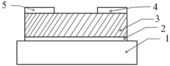
- Employing a transparent channel layer made of zinc oxide or doped zinc oxide, eliminating the need for light-blocking layers by using transparent conductive materials for the channel, source, drain, and gate electrodes, and incorporating transparent or partially transparent electrodes to enhance the aperture ratio and reduce energy consumption.
- A p-type CuNiSnO amorphous oxide semiconductor film composed of Cu, Ni and Sn elements is used. High-purity Cu2O, NiO and SnO powders are sintered in an Ar atmosphere and combined with pulse laser deposition technology to deposit on the substrate to form p-type CuNiSnO. Amorphous film, ensure that Cu is +1 valence, Ni is +2 valence, Sn is +2 valence, the chemical formula is CuxNiySnzO0.5x+y+z, 0.1≦x≦0.5, 0.1≦y≦0.5, 0.2≦z≦0.5 ,x+y+z=1.
Environmental Impact of Quasicrystal Conductor Production
The production of quasicrystal-based transparent conductors presents both opportunities and challenges in terms of environmental impact. As with any emerging technology, it is crucial to assess the potential ecological consequences throughout the entire lifecycle of these materials.
The manufacturing process of quasicrystal conductors typically involves high-temperature synthesis and precision control of material composition. This energy-intensive process may lead to increased carbon emissions compared to traditional conductor production methods. However, the unique properties of quasicrystals, such as their thermal stability and electrical conductivity, could potentially offset these initial environmental costs through improved product longevity and efficiency.
Raw material extraction for quasicrystal production is another area of environmental concern. Many quasicrystals contain rare earth elements or transition metals, which often require resource-intensive mining operations. The extraction of these materials can lead to habitat destruction, soil erosion, and water pollution if not managed responsibly. It is essential to develop sustainable sourcing practices and explore alternative material compositions that rely on more abundant elements.
The potential for recycling and reuse of quasicrystal conductors is a promising aspect of their environmental profile. Due to their stable structure and resistance to degradation, quasicrystals may be more easily recoverable from end-of-life products compared to conventional materials. This could lead to a reduction in electronic waste and promote a more circular economy in the electronics industry.
Water usage and potential contamination during the production process are additional environmental factors to consider. The synthesis and purification of quasicrystals may require significant amounts of water and potentially harmful chemicals. Implementing closed-loop water systems and developing green chemistry approaches for quasicrystal synthesis could help mitigate these impacts.
As transparent conductors, quasicrystal-based materials have the potential to enhance the efficiency of solar cells and other optoelectronic devices. This improvement in energy conversion efficiency could lead to reduced overall energy consumption and associated environmental benefits in the long term. However, a comprehensive life cycle assessment is necessary to quantify these potential gains against the environmental costs of production.
The disposal and end-of-life management of quasicrystal conductors must also be carefully considered. While their stability may be advantageous for recycling, it could also pose challenges for natural decomposition if improperly disposed of. Developing effective recycling technologies and establishing proper disposal protocols will be crucial to minimizing the long-term environmental impact of these materials.
Intellectual Property Landscape in Quasicrystal Technology
The intellectual property landscape in quasicrystal technology for transparent conductors is rapidly evolving, reflecting the growing interest and potential applications in this field. Patent filings related to quasicrystalline structures for transparent conductive materials have seen a significant increase over the past decade, with major technology companies and research institutions leading the way.
Key patent holders in this domain include multinational corporations such as Samsung, LG, and 3M, who have been actively developing quasicrystal-based transparent conductors for use in displays and touch screens. These companies have filed numerous patents covering various aspects of quasicrystal synthesis, deposition techniques, and device integration methods.
Academic institutions, particularly those in the United States, Japan, and Europe, have also made substantial contributions to the patent landscape. Universities such as MIT, Stanford, and the University of Tokyo have secured patents on novel quasicrystal compositions and fabrication processes specifically tailored for transparent conductive applications.
The patent landscape reveals several key technology clusters. One prominent area focuses on the development of quasicrystalline alloys with enhanced optical transparency and electrical conductivity. Another cluster centers on innovative deposition techniques for creating uniform quasicrystalline thin films on various substrates. Patents related to the integration of quasicrystal-based transparent conductors into flexible and stretchable electronics represent a growing trend in the field.
Geographically, the distribution of patents shows a concentration in East Asia, particularly in South Korea and Japan, followed by the United States and Europe. This distribution aligns with the regions where major display manufacturers and electronics companies are based.
Recent patent trends indicate an increasing focus on environmentally friendly and cost-effective production methods for quasicrystal-based transparent conductors. Patents addressing scalability and mass production challenges are also becoming more prevalent, signaling a shift towards commercialization efforts.
The intellectual property landscape also reveals potential areas for future innovation. These include patents targeting the development of self-assembling quasicrystalline structures, the use of AI and machine learning for optimizing quasicrystal compositions, and the exploration of hybrid materials combining quasicrystals with other advanced materials like graphene or carbon nanotubes.
As the field continues to mature, it is likely that patent disputes and licensing agreements will play an increasingly important role in shaping the competitive landscape for quasicrystal-based transparent conductors. Companies and research institutions will need to navigate this complex intellectual property environment carefully to successfully commercialize their innovations in this promising technology area.