Quasicrystal Developments in Micro-Electromechanical Systems
Quasicrystal MEMS Background and Objectives
Quasicrystals, discovered in 1982 by Dan Shechtman, represent a unique class of materials that exhibit long-range order but lack periodicity. This groundbreaking discovery challenged the conventional understanding of crystalline structures and opened up new avenues for materials science research. In recent years, the integration of quasicrystals into Micro-Electromechanical Systems (MEMS) has emerged as a promising field with potential applications across various industries.
The development of quasicrystal-based MEMS technology aims to leverage the distinctive properties of quasicrystals, such as their high hardness, low friction coefficients, and unique electronic characteristics. These properties make quasicrystals particularly attractive for enhancing the performance and durability of MEMS devices, which are crucial components in modern electronics, sensors, and actuators.
The evolution of quasicrystal MEMS technology can be traced through several key milestones. Initial research focused on understanding the fundamental properties of quasicrystals and their potential applications in MEMS. This was followed by efforts to develop fabrication techniques capable of incorporating quasicrystalline materials into microscale devices. Recent advancements have seen the successful integration of quasicrystals into various MEMS components, demonstrating improved wear resistance, thermal stability, and novel electromagnetic properties.
Current research in quasicrystal MEMS is driven by the need for miniaturization, increased functionality, and enhanced reliability in microdevices. The unique atomic arrangements of quasicrystals offer possibilities for creating MEMS with superior mechanical and electrical properties compared to traditional crystalline materials. This has led to investigations into quasicrystal-based sensors, actuators, and energy harvesting devices that could outperform their conventional counterparts.
The primary objectives of quasicrystal MEMS development include optimizing fabrication processes for large-scale production, exploring new quasicrystalline compositions tailored for specific MEMS applications, and developing innovative device designs that fully exploit the unique properties of quasicrystals. Additionally, researchers aim to overcome challenges such as integrating quasicrystals with existing MEMS materials and improving the overall system performance under various operating conditions.
As the field progresses, it is anticipated that quasicrystal MEMS technology will play a significant role in advancing next-generation microdevices for applications in aerospace, biomedical engineering, telecommunications, and energy systems. The continued exploration of quasicrystal properties and their integration into MEMS promises to unlock new functionalities and push the boundaries of what is possible in microscale engineering.
MEMS Market Demand Analysis
The MEMS (Micro-Electromechanical Systems) market has experienced significant growth in recent years, driven by the increasing demand for miniaturized and high-performance sensors and actuators across various industries. The integration of quasicrystals in MEMS technology has opened up new possibilities for enhancing device performance and expanding application areas.
In the consumer electronics sector, MEMS devices incorporating quasicrystal structures have shown potential for improving the sensitivity and accuracy of motion sensors, accelerometers, and gyroscopes used in smartphones, wearables, and gaming devices. This has led to a growing interest from major smartphone manufacturers and wearable technology companies in adopting quasicrystal-based MEMS solutions to enhance user experience and device functionality.
The automotive industry has also recognized the benefits of quasicrystal MEMS technology, particularly in advanced driver assistance systems (ADAS) and autonomous vehicles. The unique properties of quasicrystals, such as their high mechanical strength and thermal stability, make them ideal for developing robust and reliable sensors for vehicle safety systems, navigation, and engine management.
In the healthcare and medical devices sector, quasicrystal MEMS have shown promise in developing highly sensitive biosensors and microfluidic devices. The increased surface area and unique electronic properties of quasicrystalline structures enable more efficient detection of biomolecules and improved performance in lab-on-a-chip applications. This has attracted attention from medical device manufacturers and pharmaceutical companies looking to enhance diagnostic capabilities and drug delivery systems.
The aerospace and defense industries have also expressed interest in quasicrystal MEMS technology for developing advanced navigation systems, vibration sensors, and communication devices. The ability of quasicrystals to withstand extreme conditions and provide superior electromagnetic properties makes them attractive for use in harsh environments and high-performance applications.
Market analysts predict that the global MEMS market, including quasicrystal-based devices, will continue to grow at a compound annual growth rate (CAGR) of over 8% in the coming years. This growth is expected to be driven by the increasing adoption of Internet of Things (IoT) devices, smart home technologies, and industrial automation systems, all of which rely heavily on MEMS sensors and actuators.
However, challenges remain in the widespread adoption of quasicrystal MEMS technology. These include the need for more cost-effective manufacturing processes, improved integration with existing MEMS fabrication techniques, and further research to fully exploit the unique properties of quasicrystals in MEMS applications. Addressing these challenges will be crucial for realizing the full market potential of quasicrystal MEMS devices across various industries.
Quasicrystal MEMS Current Status and Challenges
The integration of quasicrystals into Micro-Electromechanical Systems (MEMS) represents a frontier in materials science and engineering. Currently, the field is characterized by both significant advancements and persistent challenges. Quasicrystals, with their unique aperiodic atomic structures, offer promising properties for MEMS applications, including high hardness, low friction, and thermal stability.
One of the primary challenges in quasicrystal MEMS development is the difficulty in fabricating large-scale, defect-free quasicrystalline structures. Traditional MEMS manufacturing techniques often struggle to maintain the precise atomic arrangements necessary for quasicrystalline properties. Researchers are exploring advanced deposition methods, such as molecular beam epitaxy and pulsed laser deposition, to overcome these limitations.
Another significant hurdle is the integration of quasicrystals with existing MEMS materials and processes. The unique electronic and mechanical properties of quasicrystals can lead to compatibility issues with conventional MEMS components. This necessitates the development of novel interface materials and fabrication techniques to ensure seamless integration without compromising the quasicrystalline structure.
The characterization and modeling of quasicrystal behavior in MEMS environments present additional challenges. The complex atomic structure of quasicrystals makes traditional modeling approaches less effective, requiring the development of new computational methods to accurately predict their performance in MEMS devices.
Despite these challenges, significant progress has been made in recent years. Researchers have successfully demonstrated quasicrystal-based MEMS sensors with enhanced sensitivity and stability. The use of quasicrystalline coatings in MEMS actuators has shown promise in reducing wear and improving efficiency.
Geographically, research in quasicrystal MEMS is concentrated in a few key regions. Japan and Germany lead in fundamental quasicrystal research, while the United States and China are at the forefront of MEMS integration efforts. Collaborative international projects are becoming increasingly common, fostering knowledge exchange and accelerating progress in the field.
Looking ahead, the development of scalable manufacturing processes for quasicrystal MEMS remains a critical challenge. Researchers are exploring novel approaches, including 3D printing and self-assembly techniques, to overcome current fabrication limitations. Additionally, efforts are underway to expand the range of quasicrystalline materials suitable for MEMS applications, potentially opening new avenues for device design and functionality.
Current Quasicrystal MEMS Solutions
01 Synthesis and production of quasicrystals
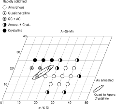
Methods for synthesizing and producing quasicrystalline materials, including techniques for controlling composition, structure, and properties. This involves specific processing conditions, alloying methods, and rapid solidification techniques to create stable quasicrystalline phases.- Synthesis and production of quasicrystals: Methods for synthesizing and producing quasicrystalline materials, including techniques for controlling composition, structure, and properties. This may involve specific alloying processes, heat treatments, or rapid solidification techniques to achieve the unique aperiodic atomic arrangements characteristic of quasicrystals.
- Applications of quasicrystals in coatings and surface treatments: Utilization of quasicrystalline materials in coatings and surface treatments to enhance properties such as wear resistance, corrosion protection, and non-stick characteristics. This includes methods for applying quasicrystalline coatings to various substrates and their use in specific industrial applications.
- Quasicrystal-based composites and alloys: Development of composite materials and alloys incorporating quasicrystalline phases to achieve improved mechanical, thermal, or electrical properties. This may include methods for dispersing quasicrystalline particles in metal matrices or creating bulk quasicrystalline alloys with enhanced characteristics.
- Optical and photonic applications of quasicrystals: Exploration of quasicrystals in optical and photonic devices, leveraging their unique structural properties for applications such as light manipulation, photonic bandgap materials, or novel optical coatings. This includes the design and fabrication of quasicrystalline structures for specific optical functions.
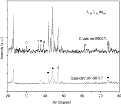
- Characterization and analysis techniques for quasicrystals: Methods and tools for analyzing and characterizing quasicrystalline materials, including advanced microscopy techniques, diffraction analysis, and computational modeling. These approaches help in understanding the unique structural and physical properties of quasicrystals, aiding in their further development and application.
02 Applications of quasicrystals in coatings and surface treatments
Utilization of quasicrystalline materials in coatings and surface treatments to enhance properties such as wear resistance, corrosion protection, and thermal insulation. This includes methods for applying quasicrystalline coatings to various substrates and their use in specific industrial applications.Expand Specific Solutions03 Quasicrystal-based composites and alloys
Development of composite materials and alloys incorporating quasicrystalline phases to achieve unique combinations of properties. This includes methods for creating bulk quasicrystalline materials, reinforcing conventional alloys with quasicrystalline particles, and designing novel material systems with enhanced performance characteristics.Expand Specific Solutions04 Optical and photonic applications of quasicrystals
Exploration of quasicrystals in optical and photonic devices, leveraging their unique structural properties for applications such as light manipulation, photonic bandgap materials, and novel optical coatings. This includes the design and fabrication of quasicrystalline structures for specific optical functionalities.Expand Specific Solutions05 Characterization and analysis techniques for quasicrystals
Advanced methods for characterizing and analyzing quasicrystalline materials, including electron microscopy, X-ray diffraction, and computational modeling techniques. These approaches enable the study of quasicrystal structure, composition, and properties at various scales, facilitating the understanding and optimization of quasicrystalline materials.Expand Specific Solutions
Key Players in Quasicrystal MEMS Industry
The field of quasicrystal developments in Micro-Electromechanical Systems (MEMS) is in an emerging stage, with growing market potential as researchers explore novel applications. The global MEMS market is projected to reach significant size, driven by increasing demand in various industries. Technological maturity varies, with institutions like Massachusetts Institute of Technology, University of California, and Nanjing University leading academic research. Companies such as NXP Semiconductors, Samsung Electronics, and Siemens are actively developing commercial applications. The competition landscape is diverse, involving both academic institutions and industry players, indicating a collaborative yet competitive environment for innovation in quasicrystal-based MEMS technologies.
Sony Group Corp.
Samsung Electronics Co., Ltd.
Core Quasicrystal MEMS Patents and Literature
- A polyhedral quasicrystalline material with long-range translational order and rotational symmetry is used in the phase change layer, enabling phase transitions between quasi-crystalline and crystalline states with minimal energy change, allowing for fast phase transitions.
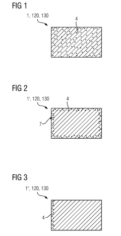
- Incorporating quasi-crystal particles into metal alloys, which have tunable properties between metals and ceramics, minimizing thermal stresses and enhancing mechanical strength, abrasion resistance, and providing thermal insulation through controlled surface concentration gradients.
Material Science Advancements for Quasicrystals
Recent advancements in material science have significantly propelled the development of quasicrystals, particularly in their application to Micro-Electromechanical Systems (MEMS). The unique structural properties of quasicrystals, characterized by their aperiodic yet ordered atomic arrangements, have opened new avenues for enhancing the performance and functionality of MEMS devices.
One of the key breakthroughs in this field has been the successful synthesis of stable quasicrystalline thin films. These films exhibit exceptional mechanical properties, including high hardness and low friction coefficients, making them ideal for use in MEMS components subject to wear and tear. The development of novel deposition techniques, such as molecular beam epitaxy and pulsed laser deposition, has enabled precise control over the growth of these films, allowing for tailored properties at the nanoscale.
Furthermore, researchers have made significant progress in understanding the electronic properties of quasicrystals. The discovery of unique electron localization patterns in quasicrystalline structures has led to the development of novel sensors and actuators with enhanced sensitivity and responsiveness. This has particularly benefited MEMS devices used in environmental monitoring and biomedical applications.
The thermal properties of quasicrystals have also been extensively studied and exploited in MEMS design. Their low thermal conductivity, coupled with high thermal stability, makes them excellent candidates for thermal management in miniaturized devices. This has led to the development of more efficient micro-heaters and thermal insulators, crucial for the performance of many MEMS-based systems.
Another significant advancement has been in the area of surface engineering. The complex surface structures of quasicrystals have been harnessed to create superhydrophobic and self-cleaning surfaces, which are particularly valuable in microfluidic MEMS devices. These surfaces exhibit remarkable resistance to fouling and contamination, enhancing the longevity and reliability of MEMS components in harsh environments.
The integration of quasicrystals with other advanced materials, such as graphene and carbon nanotubes, has opened up new possibilities for hybrid MEMS structures. These composites combine the unique properties of quasicrystals with the exceptional mechanical and electrical characteristics of nanomaterials, leading to MEMS devices with unprecedented performance metrics.
Lastly, computational materials science has played a crucial role in advancing quasicrystal research for MEMS applications. Advanced modeling techniques, including density functional theory and molecular dynamics simulations, have provided deep insights into the behavior of quasicrystals at atomic and molecular levels. This has accelerated the design and optimization of quasicrystal-based MEMS components, reducing development time and costs.
Quasicrystal MEMS Fabrication Techniques
The fabrication of quasicrystal-based Micro-Electromechanical Systems (MEMS) presents unique challenges and opportunities in the field of advanced materials and microfabrication. Traditional MEMS fabrication techniques must be adapted and refined to accommodate the complex structures and properties of quasicrystals.
One of the primary fabrication methods for quasicrystal MEMS is thin film deposition. This process typically involves physical vapor deposition (PVD) techniques such as sputtering or electron beam evaporation. These methods allow for precise control over film thickness and composition, which is crucial for maintaining the unique quasicrystalline structure. However, achieving the correct stoichiometry and phase formation can be challenging, often requiring careful optimization of deposition parameters and post-deposition annealing processes.
Lithography plays a critical role in patterning quasicrystal MEMS structures. Both photolithography and electron beam lithography have been employed, with the latter offering higher resolution for nanoscale features. The non-periodic nature of quasicrystals necessitates advanced pattern generation algorithms to accurately reproduce their complex geometries.
Etching techniques for quasicrystal MEMS must be carefully selected to preserve the material's unique properties. Wet etching methods are often limited due to the chemical complexity of quasicrystals. Dry etching techniques, such as reactive ion etching (RIE) or focused ion beam (FIB) milling, have shown promise in achieving high-aspect-ratio structures while maintaining material integrity.
Surface micromachining has been adapted for quasicrystal MEMS fabrication, allowing for the creation of suspended structures and movable components. This process typically involves the deposition and selective removal of sacrificial layers, with careful consideration given to material compatibility and etch selectivity.
Integration of quasicrystals with conventional MEMS materials presents additional challenges. Techniques such as wafer bonding and selective area growth have been explored to combine quasicrystalline elements with silicon or other standard MEMS substrates. These hybrid approaches aim to leverage the unique properties of quasicrystals while maintaining compatibility with established MEMS fabrication processes.
Post-processing steps, including thermal annealing and surface treatments, are often necessary to optimize the performance of quasicrystal MEMS devices. These processes can enhance structural stability, improve electrical properties, and refine surface characteristics for specific applications.
As research in this field progresses, novel fabrication techniques continue to emerge. These include additive manufacturing methods adapted for microscale quasicrystalline structures and advanced epitaxial growth techniques for creating highly ordered quasicrystal thin films. The ongoing development of these fabrication methods is crucial for realizing the full potential of quasicrystal-based MEMS devices in various applications, from sensors and actuators to energy harvesting systems.
