Quasicrystal and Semiconductor Integration Benefits
Quasicrystal-Semiconductor Integration Background
The integration of quasicrystals and semiconductors represents a fascinating frontier in materials science and engineering. Quasicrystals, discovered in 1982 by Dan Shechtman, are unique structures that exhibit long-range order but lack periodicity. This distinctive arrangement of atoms results in properties that differ significantly from those of traditional crystalline materials. On the other hand, semiconductors have been the cornerstone of modern electronics for decades, powering everything from smartphones to solar panels.
The convergence of these two fields has sparked considerable interest in the scientific community due to the potential for novel applications and enhanced performance in electronic devices. Quasicrystals offer unique electronic, thermal, and optical properties that could complement or enhance the capabilities of conventional semiconductors. For instance, the aperiodic nature of quasicrystals can lead to unusual electronic band structures, potentially opening up new avenues for tailoring electronic properties.
One of the primary motivations for exploring quasicrystal-semiconductor integration is the possibility of overcoming certain limitations inherent in traditional semiconductor materials. As the demand for smaller, faster, and more efficient electronic devices continues to grow, the semiconductor industry faces challenges in scaling down conventional technologies. Quasicrystals, with their distinct structural and electronic characteristics, may offer solutions to some of these challenges.
The integration process itself presents numerous technical hurdles. Quasicrystals and semiconductors have fundamentally different atomic structures and formation mechanisms, making their seamless combination a complex task. Researchers are exploring various methods to achieve this integration, including thin film deposition, epitaxial growth, and nanostructure fabrication. Each approach comes with its own set of challenges and potential benefits.
Furthermore, the study of quasicrystal-semiconductor interfaces is crucial for understanding and optimizing their combined properties. These interfaces can exhibit unique phenomena due to the interaction between the quasiperiodic structure of the quasicrystal and the periodic lattice of the semiconductor. Such interactions could lead to novel electronic states or improved charge carrier dynamics.
As research in this field progresses, scientists and engineers are also investigating the potential applications of quasicrystal-semiconductor hybrid systems. These could range from more efficient thermoelectric devices and improved photovoltaic cells to novel quantum computing architectures and advanced sensing technologies. The unique properties of quasicrystals, such as their low thermal conductivity and unusual electronic structure, could be leveraged to enhance the performance of semiconductor-based devices in ways previously thought impossible.
Market Potential Analysis
The integration of quasicrystals with semiconductors presents a promising market opportunity in the advanced materials and electronics sectors. This novel combination has the potential to revolutionize various applications, particularly in the fields of optoelectronics, photonics, and high-performance computing.
The global semiconductor market, valued at approximately $556 billion in 2021, is projected to grow significantly in the coming years. The integration of quasicrystals into semiconductor technologies could capture a substantial portion of this market, especially in niche applications that require unique electronic and optical properties.
One of the primary drivers for market demand is the potential for improved energy efficiency in electronic devices. Quasicrystal-semiconductor hybrids may offer superior thermal management properties, which could lead to reduced power consumption and extended battery life in portable electronics. This aligns with the growing consumer demand for longer-lasting, more energy-efficient devices.
In the telecommunications sector, the unique light-manipulating properties of quasicrystals could enhance the performance of optical components used in fiber-optic networks. As global data traffic continues to surge, the demand for faster and more efficient data transmission technologies is expected to grow, creating a significant market opportunity for quasicrystal-enhanced photonic devices.
The automotive industry represents another potential market for quasicrystal-semiconductor integration. With the increasing adoption of electric vehicles and advanced driver assistance systems, there is a growing need for high-performance, energy-efficient electronic components. Quasicrystal-based semiconductors could provide the necessary improvements in power management and sensor technologies required for these applications.
In the realm of quantum computing, quasicrystals' unique electronic properties may offer advantages in developing more stable and efficient qubits. As investment in quantum technologies continues to rise, this could open up a highly specialized but potentially lucrative market segment for quasicrystal-semiconductor hybrid materials.
The aerospace and defense sectors also present significant market potential. The enhanced thermal stability and radiation resistance of quasicrystal-semiconductor materials could prove valuable in developing more robust electronic systems for satellites, spacecraft, and military applications.
However, it is important to note that the market for quasicrystal-semiconductor integration is still in its early stages. Significant research and development efforts will be required to fully realize the commercial potential of these materials. The initial market adoption is likely to focus on high-value, specialized applications where the unique properties of quasicrystals can justify the potentially higher production costs.
As manufacturing processes improve and economies of scale are achieved, the market potential for quasicrystal-semiconductor integration is expected to expand into more mainstream applications. This could lead to a gradual but significant shift in the semiconductor industry, potentially creating new market leaders and disrupting existing supply chains.
Current Challenges and Limitations
The integration of quasicrystals with semiconductors presents several significant challenges and limitations that researchers and engineers must overcome. One of the primary obstacles is the fundamental structural incompatibility between quasicrystals and traditional semiconductor materials. Quasicrystals possess a unique aperiodic atomic structure, which contrasts sharply with the periodic lattice structure of conventional semiconductors. This mismatch makes it difficult to achieve seamless integration without compromising the properties of either material.
Another major challenge lies in the growth and fabrication processes. Quasicrystals typically require specific growth conditions that differ substantially from those used in semiconductor manufacturing. The precise control of temperature, pressure, and composition needed to form quasicrystalline structures is often incompatible with standard semiconductor fabrication techniques. This incompatibility leads to difficulties in creating hybrid structures or interfaces between quasicrystals and semiconductors without introducing defects or impurities.
The electronic properties of quasicrystals pose additional challenges for integration. While semiconductors have well-defined band structures that enable controlled electrical behavior, quasicrystals exhibit complex electronic states that are not fully understood. This lack of understanding makes it challenging to predict and control the electronic interactions at the interface between quasicrystals and semiconductors, potentially limiting the functionality of integrated devices.
Thermal management is another critical issue in quasicrystal-semiconductor integration. Quasicrystals often have different thermal expansion coefficients compared to semiconductors, which can lead to stress and strain at the interface during temperature fluctuations. This thermal mismatch may result in mechanical instability, delamination, or the formation of defects that degrade device performance over time.
Furthermore, the limited availability of high-quality quasicrystalline materials in large quantities and with consistent properties presents a significant barrier to large-scale integration. The synthesis of quasicrystals with the purity and structural perfection required for semiconductor applications remains challenging and costly, hindering their widespread adoption in the semiconductor industry.
Characterization and quality control of quasicrystal-semiconductor interfaces also pose substantial challenges. Traditional analytical techniques used in semiconductor manufacturing may not be directly applicable to quasicrystalline structures, necessitating the development of new methods for assessing the quality and performance of integrated devices. This lack of established characterization protocols makes it difficult to ensure consistent and reliable integration outcomes.
Lastly, the current limitations in theoretical modeling and simulation tools for quasicrystalline structures impede the rapid development and optimization of integrated quasicrystal-semiconductor devices. The complex nature of quasicrystals requires advanced computational methods that can accurately predict their behavior when interfaced with semiconductors, a capability that is still evolving in the scientific community.
Existing Integration Approaches
01 Synthesis and production of quasicrystals
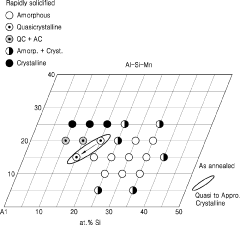
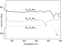
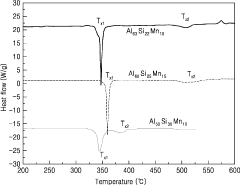
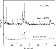
Various methods for synthesizing and producing quasicrystals, including rapid solidification techniques, melt spinning, and vapor deposition. These processes involve precise control of composition, temperature, and cooling rates to achieve the unique atomic structure of quasicrystals.- Synthesis and production of quasicrystals: Methods for synthesizing and producing quasicrystalline materials, including techniques for controlling composition, structure, and properties. This involves specific processing conditions, alloying methods, and rapid solidification techniques to create stable quasicrystalline phases.
- Applications of quasicrystals in coatings and surface treatments: Utilization of quasicrystalline materials in coatings and surface treatments to enhance properties such as wear resistance, corrosion protection, and thermal insulation. This includes methods for applying quasicrystalline coatings to various substrates and their use in specific industrial applications.
- Quasicrystal-based composites and alloys: Development of composite materials and alloys incorporating quasicrystalline phases to achieve unique combinations of properties. This involves designing and fabricating materials with improved mechanical, thermal, or electrical characteristics by leveraging the unique structure of quasicrystals.
- Optical and photonic applications of quasicrystals: Exploration of quasicrystals in optical and photonic devices, leveraging their unique structural properties for applications such as light manipulation, photonic bandgap materials, and novel optical coatings. This includes the design and fabrication of quasicrystal-based optical components.
- Characterization and analysis techniques for quasicrystals: Advanced methods for characterizing and analyzing quasicrystalline materials, including electron microscopy, X-ray diffraction, and computational modeling techniques. These approaches enable better understanding of quasicrystal structure, composition, and properties for research and industrial applications.
02 Applications of quasicrystals in materials science
Quasicrystals have unique properties that make them valuable in various applications, such as low-friction coatings, thermal barriers, and reinforcement in composite materials. Their unusual atomic structure contributes to improved wear resistance, thermal insulation, and mechanical strength.Expand Specific Solutions03 Optical properties and photonic applications of quasicrystals
Quasicrystals exhibit interesting optical properties due to their aperiodic structure, including photonic band gaps and unusual light transmission characteristics. These properties make them suitable for applications in optical devices, sensors, and photonic crystals.Expand Specific Solutions04 Characterization and analysis of quasicrystalline structures
Advanced techniques for characterizing and analyzing quasicrystalline structures, including electron microscopy, X-ray diffraction, and computational modeling. These methods help in understanding the unique atomic arrangements and properties of quasicrystals.Expand Specific Solutions05 Novel quasicrystalline alloys and compositions
Development of new quasicrystalline alloys and compositions with enhanced properties or specific functionalities. This includes the exploration of different elemental combinations and processing conditions to create quasicrystals with tailored characteristics for various applications.Expand Specific Solutions
Key Industry Players and Competitors
The integration of quasicrystals and semiconductors is an emerging field in the early stages of development, with a growing market potential as researchers explore novel applications. The technology's maturity is still relatively low, with leading institutions like Massachusetts Institute of Technology, Taiwan Semiconductor Manufacturing Co., Ltd., and Samsung Electronics Co., Ltd. at the forefront of research. The market size is currently limited but expected to expand as the technology progresses. Key players such as ChangXin Memory Technologies, Inc. and Nexchip Semiconductor Corp. are investing in R&D to leverage the unique properties of quasicrystals for enhancing semiconductor performance. As the technology matures, it could potentially disrupt traditional semiconductor manufacturing processes, attracting interest from major industry players and research institutions worldwide.
Massachusetts Institute of Technology
Taiwan Semiconductor Manufacturing Co., Ltd.
Breakthrough Innovations in Integration
- A polyhedral quasicrystalline material with long-range translational order and rotational symmetry is used in the phase change layer, enabling phase transitions between quasi-crystalline and crystalline states with minimal energy change, allowing for fast phase transitions.
- The development of interconnect structures that integrate superconducting qubit ICs through an active or passive superconducting base, enabling 3D integration to optimize cryogenic space usage, increase integration density, and enhance functionality, using multi-layer semiconductor structures with superconducting and conductive materials like Titanium, Platinum, Gold, and Indium for efficient coupling and bonding.
Material Compatibility and Fabrication Techniques
The integration of quasicrystals with semiconductors presents unique challenges and opportunities in terms of material compatibility and fabrication techniques. Quasicrystals, with their aperiodic long-range order, exhibit distinct physical and chemical properties that differ significantly from traditional crystalline materials used in semiconductor manufacturing.
One of the primary challenges in integrating quasicrystals with semiconductors lies in the structural mismatch between the two materials. Semiconductors typically have a periodic crystal structure, while quasicrystals lack translational symmetry. This fundamental difference necessitates innovative approaches to achieve seamless integration without compromising the desirable properties of either material.
Material compatibility issues also arise from the chemical composition of quasicrystals, which often include elements not commonly used in semiconductor fabrication. For instance, many quasicrystals contain aluminum, which can introduce unwanted impurities in silicon-based semiconductors. Developing strategies to mitigate these potential contamination issues is crucial for successful integration.
Fabrication techniques for quasicrystal-semiconductor hybrid structures require significant adaptation of existing semiconductor manufacturing processes. Traditional methods such as chemical vapor deposition (CVD) or molecular beam epitaxy (MBE) may not be directly applicable due to the unique growth conditions required for quasicrystals. Novel deposition techniques, such as pulsed laser deposition or sputtering, have shown promise in creating thin films of quasicrystalline materials on semiconductor substrates.
Interface engineering plays a critical role in ensuring proper adhesion and electrical contact between quasicrystals and semiconductors. Techniques such as buffer layer growth or surface modification may be necessary to promote compatibility and reduce interfacial defects. Additionally, controlling the orientation relationship between the quasicrystal and semiconductor layers is essential for optimizing device performance.
Post-deposition processing of quasicrystal-semiconductor structures presents another set of challenges. Conventional annealing and etching processes may need to be modified to preserve the unique structure of quasicrystals while achieving desired semiconductor properties. Developing selective etching techniques that can differentiate between quasicrystalline and crystalline regions is particularly important for device fabrication.
Despite these challenges, recent advancements in nanofabrication techniques offer new possibilities for quasicrystal-semiconductor integration. For example, focused ion beam milling and electron beam lithography enable precise patterning of quasicrystalline structures on semiconductor surfaces, opening avenues for novel device architectures.
Quantum Computing Applications
Quantum computing applications in the field of quasicrystals and semiconductor integration offer promising avenues for advancing both theoretical understanding and practical implementations. The unique properties of quasicrystals, such as their aperiodic long-range order and unusual symmetries, present intriguing possibilities for quantum information processing and quantum simulation.
One potential application lies in the development of quantum sensors based on quasicrystalline structures. The non-periodic nature of quasicrystals can be exploited to create highly sensitive detectors for magnetic fields, electric fields, and other physical quantities. These sensors could potentially outperform traditional semiconductor-based sensors in certain applications, particularly in environments with high levels of noise or interference.
Quantum computing algorithms could also be leveraged to simulate and study the complex electronic and structural properties of quasicrystals. This approach may lead to new insights into the formation and stability of quasicrystalline phases, as well as their potential applications in materials science and engineering. Furthermore, quantum simulations could aid in the design of novel quasicrystal-semiconductor hybrid materials with tailored electronic and optical properties.
The integration of quasicrystals with semiconductor technologies opens up possibilities for creating unique quantum devices. For instance, quasicrystalline structures could be used to create novel quantum dot arrays or photonic crystals with unconventional band structures. These structures may exhibit interesting quantum confinement effects and could potentially be used in quantum information processing or quantum communication applications.
Another promising area of research is the use of quantum computing techniques to optimize the growth and fabrication processes for quasicrystal-semiconductor heterostructures. Quantum algorithms could be employed to predict optimal growth conditions, interface properties, and defect formation, leading to improved control over the integration process and enhanced device performance.
Quantum error correction schemes could also benefit from the unique properties of quasicrystals. The aperiodic nature of quasicrystalline structures may offer new approaches to designing quantum error-correcting codes with improved resilience against decoherence and other sources of noise in quantum systems.
In conclusion, the intersection of quantum computing, quasicrystals, and semiconductor integration presents a rich landscape for scientific exploration and technological innovation. As quantum computing capabilities continue to advance, we can expect to see increasingly sophisticated applications in this interdisciplinary field, potentially leading to breakthroughs in materials science, quantum information processing, and beyond.