How to Optimize RRAM for Increased Data Density
SEP 10, 20259 MIN READ
Generate Your Research Report Instantly with AI Agent
Patsnap Eureka helps you evaluate technical feasibility & market potential.
RRAM Technology Evolution and Optimization Goals
Resistive Random Access Memory (RRAM) has emerged as a promising non-volatile memory technology over the past two decades, evolving from theoretical concepts to commercial implementations. The technology leverages the resistance switching phenomenon in certain metal oxides and other materials to store binary information. This evolution has been driven by the increasing demand for higher storage density, lower power consumption, and faster access times in memory technologies.
The initial development of RRAM began in the early 2000s when researchers observed reliable resistance switching in various oxide materials. By 2010, significant progress had been made in understanding the underlying mechanisms, particularly the formation and rupture of conductive filaments within the switching layer. This fundamental understanding paved the way for more sophisticated device architectures and material systems.
From 2010 to 2015, RRAM technology advanced from single-cell demonstrations to small arrays, with improvements in endurance, retention, and switching speed. The period from 2015 to 2020 saw the emergence of 3D architectures and multi-level cell capabilities, significantly enhancing storage density. Recent developments have focused on improving reliability, reducing variability, and scaling down device dimensions to nanometer ranges.
Current RRAM technology faces several optimization challenges that must be addressed to achieve higher data density. These include reducing cell-to-cell variability, enhancing multi-level cell stability, minimizing sneak path currents in crossbar arrays, and improving the endurance of devices under repeated programming cycles. The trade-off between retention time and switching speed also remains a significant challenge.
The primary optimization goals for RRAM technology include achieving reliable multi-bit storage per cell (beyond 2 bits), reducing the cell size below 10nm without compromising performance, developing more efficient selector devices for high-density arrays, and improving programming algorithms to enhance endurance beyond 10^9 cycles. Additionally, there is a focus on reducing the energy consumption per bit to below 1pJ.
Material engineering represents another critical aspect of RRAM optimization, with research directed toward novel switching materials, electrode combinations, and interface engineering to enhance performance metrics. Hybrid approaches that combine RRAM with other emerging memory technologies are also being explored to leverage complementary advantages.
The ultimate goal is to position RRAM as a universal memory solution that combines the speed of SRAM, the density of NAND flash, and the non-volatility of storage-class memory. This would enable new computing paradigms, including in-memory computing and neuromorphic applications, potentially revolutionizing the memory hierarchy in computing systems.
Market Demand Analysis for High-Density Memory Solutions
The global memory market is experiencing unprecedented demand for high-density storage solutions, driven primarily by the explosive growth in data-intensive applications. Current projections indicate the high-performance memory market will reach $125 billion by 2026, with a compound annual growth rate of 23%. Within this landscape, RRAM (Resistive Random Access Memory) technology represents a particularly promising segment due to its potential for ultra-high density storage capabilities.
Data centers and cloud computing infrastructure providers constitute the largest market segment seeking advanced memory solutions. These entities face mounting pressure to store and process exponentially growing volumes of data while minimizing physical footprint and energy consumption. RRAM's theoretical ability to achieve multi-bit storage per cell directly addresses this critical need, potentially offering 3-4 times higher data density than conventional flash memory.
The artificial intelligence and machine learning sector presents another significant market opportunity. Training sophisticated AI models requires massive datasets and high-speed memory access. Market research indicates that 78% of enterprise AI developers cite memory constraints as a primary bottleneck in model development. RRAM's combination of high density and relatively fast access times positions it as an ideal candidate for AI acceleration hardware.
Mobile device manufacturers represent the third major market segment. Consumer expectations for smartphone storage capacity have increased by approximately 40% annually over the past five years, while device dimensions remain constrained. This contradiction creates strong demand for memory solutions that can pack more data into the same or smaller physical space. RRAM's potential for vertical stacking and 3D integration aligns perfectly with these requirements.
The automotive industry, particularly the autonomous vehicle segment, is emerging as a new frontier for high-density memory applications. Self-driving systems generate up to 4TB of data per day of operation, necessitating robust onboard storage solutions. The harsh operating conditions of automotive environments also favor RRAM's superior temperature stability compared to conventional memory technologies.
Edge computing applications represent another growth vector, with IoT deployments expected to reach 75 billion connected devices by 2025. These distributed systems require local storage solutions that combine high density with low power consumption – precisely the attributes that optimized RRAM technology promises to deliver.
Market analysis reveals that customers across these segments are willing to pay a premium of 15-20% for memory solutions that deliver substantial density improvements, creating a clear economic incentive for continued RRAM optimization research and development.
Current RRAM Limitations and Technical Challenges
Despite significant advancements in RRAM technology, several critical limitations continue to impede its optimization for increased data density. The foremost challenge is the inherent variability in resistive switching behavior, which manifests as inconsistent resistance states across different memory cells and even within the same cell over multiple programming cycles. This stochastic nature of filament formation and rupture processes creates reliability issues that severely constrain the implementation of multi-level cell (MLC) architectures necessary for higher data density.
The sneak path current problem presents another significant obstacle, particularly in crossbar array structures. As array density increases, parasitic currents through unselected cells create read disturbances and power consumption issues, ultimately limiting the practical size and density of RRAM arrays. Current selector devices add complexity and area overhead, counteracting density improvements.
Endurance limitations also pose substantial challenges, with most RRAM devices exhibiting performance degradation after 10^6-10^9 write cycles. This degradation stems from physical and chemical changes in the switching material, including electrode metal diffusion, oxygen vacancy redistribution, and structural defects accumulation. For high-density storage applications requiring frequent writes, these endurance limitations become particularly problematic.
The retention-write speed trade-off represents another fundamental constraint. Materials and structures that enable fast switching typically demonstrate poorer data retention characteristics. This inverse relationship complicates the design of high-density RRAM that must simultaneously maintain data integrity and support rapid operations.
Scaling issues emerge as cell dimensions approach sub-10nm regimes. At these dimensions, quantum effects and statistical variations in material composition become increasingly pronounced, leading to greater device-to-device variability. The minimum current required for reliable switching does not scale proportionally with cell size, creating power density challenges at extreme scaling.
Manufacturing integration challenges further complicate density optimization. Many promising RRAM materials and structures remain difficult to integrate with standard CMOS processes. Issues include thermal budget constraints, material compatibility problems, and complex deposition requirements for ultra-thin films with precise stoichiometry control.
Energy efficiency concerns also limit density scaling, as the power required for write operations in RRAM remains relatively high compared to some competing technologies. This energy consumption creates thermal management challenges that become more acute as cell density increases, potentially leading to reliability issues and accelerated aging.
Current Approaches to RRAM Data Density Enhancement
01 Multi-level cell technology for increased data density
RRAM devices can be designed with multi-level cell (MLC) capabilities, allowing each memory cell to store multiple bits of information rather than just binary states. This significantly increases the data storage density without increasing the physical footprint of the memory array. MLC RRAM achieves this by precisely controlling the resistance states of the memory cell, creating multiple distinguishable resistance levels that represent different data values.- Multi-level cell technology for increased data density: RRAM devices can be designed with multi-level cell (MLC) capabilities, allowing each memory cell to store multiple bits of information rather than just binary states. This significantly increases the data storage density without increasing the physical footprint of the memory array. By precisely controlling the resistance states of the memory cell, multiple distinct resistance levels can be achieved, enabling higher information density per cell.
- 3D stacking architecture for enhanced data density: Three-dimensional stacking of RRAM cells enables dramatic increases in data density by building memory arrays vertically rather than just horizontally. This architecture allows for multiple layers of memory cells to be fabricated on top of each other, significantly multiplying the storage capacity within the same chip area. Various approaches include vertical RRAM arrays, cross-point structures, and multi-layer integration techniques that maximize the effective use of the available silicon real estate.
- Novel materials and interfaces for higher density RRAM: Advanced material engineering plays a crucial role in enhancing RRAM data density. By utilizing specialized switching materials, electrode compositions, and interface engineering, the physical size of individual memory cells can be reduced while maintaining reliable switching characteristics. Materials such as metal oxides, chalcogenides, and two-dimensional materials enable smaller feature sizes and better control over the resistive switching mechanism, leading to higher density memory arrays.
- Crossbar array architecture for maximizing data density: Crossbar array configurations represent an efficient approach to organizing RRAM cells to achieve maximum data density. In this architecture, memory cells are positioned at the intersection points of perpendicular word and bit lines, creating a highly compact memory array. This arrangement minimizes the overhead circuitry required per cell and allows for extremely dense packing of memory elements, significantly increasing the overall storage capacity per unit area.
- Scaling and fabrication techniques for ultra-high density: Advanced fabrication methods and scaling techniques are essential for pushing RRAM data density to its theoretical limits. These include sub-nanometer fabrication processes, innovative cell selector technologies, and integration with complementary metal-oxide-semiconductor (CMOS) technology. By addressing challenges such as sneak path currents and reducing the minimum feature size of memory cells, these techniques enable the creation of ultra-high density RRAM arrays suitable for next-generation storage applications.
02 3D stacking and vertical architecture
Three-dimensional stacking techniques enable dramatic increases in RRAM data density by arranging memory cells vertically rather than just in a planar configuration. These 3D architectures include cross-point arrays, vertical RRAM structures, and multi-layer stacking approaches that maximize the number of memory cells per unit area. The vertical integration allows for higher capacity without expanding the chip's horizontal dimensions, making it particularly valuable for space-constrained applications.Expand Specific Solutions03 Novel materials and interface engineering
Advanced material combinations and interface engineering techniques are employed to enhance RRAM data density. This includes using specialized switching materials, electrode materials, and barrier layers that enable smaller cell sizes while maintaining reliable switching behavior. Innovations in material science allow for reduced cell dimensions, tighter packing density, and improved performance characteristics such as lower power consumption and faster switching speeds.Expand Specific Solutions04 Scaling and miniaturization techniques
Various scaling and miniaturization approaches are implemented to reduce the physical dimensions of RRAM cells while maintaining their functionality. These techniques include advanced lithography methods, self-aligned fabrication processes, and innovative cell designs that minimize the area required per memory element. By shrinking the cell size, more memory elements can be integrated into the same chip area, directly increasing the data density of RRAM devices.Expand Specific Solutions05 Hybrid memory architectures and system integration
Hybrid memory architectures combine RRAM with other memory technologies or computing elements to optimize overall system data density. These approaches include integrating RRAM with logic circuits, using RRAM as part of neuromorphic computing systems, or combining RRAM with other memory types in heterogeneous memory systems. Such integration enables more efficient use of chip area and can increase effective data density through optimized memory hierarchies and data management techniques.Expand Specific Solutions
Leading Companies and Research Institutions in RRAM Field
The RRAM optimization for increased data density market is in a growth phase, with significant potential as memory technologies evolve beyond traditional NAND and DRAM. The global market is projected to expand substantially as RRAM offers advantages in power consumption, speed, and scalability. Technologically, the field shows varying maturity levels across key players. Industry leaders like Samsung, Huawei, and IBM are making substantial R&D investments, while specialized companies like Ovonyx Memory Technology focus exclusively on resistive memory solutions. TSMC and GlobalFoundries are developing manufacturing processes to support commercial viability. Academic-industry partnerships involving institutions like Chuo University and Industrial Technology Research Institute are accelerating innovation, particularly in materials science and device architecture to overcome current density limitations.
International Business Machines Corp.
Technical Solution: IBM has developed a unique approach to RRAM density optimization through their phase-change memory (PCM) technology, which they've evolved into a specialized form of RRAM. Their solution employs multi-level cell architecture that stores 3 bits per cell, achieving 8 distinct resistance states in a single memory element. IBM's technology utilizes a proprietary selector device integrated with each memory cell to minimize sneak path currents, allowing for denser array configurations without performance degradation. They've pioneered the use of carbon-doped GST (germanium-antimony-tellurium) materials that provide better thermal stability and resistance state retention. IBM has also developed advanced programming algorithms that use iterative write-and-verify techniques to precisely control resistance states, enabling reliable multi-bit storage even as cell dimensions shrink to sub-20nm nodes. Their research has demonstrated functional arrays with densities exceeding 4Gb/cm², representing significant advancement in RRAM data density.
Strengths: Superior multi-level cell technology with proven reliability, advanced materials science expertise, and sophisticated programming algorithms that maximize density while maintaining performance. Weaknesses: Higher power consumption during write operations compared to some competing technologies, and more complex manufacturing processes that may impact production costs.
Taiwan Semiconductor Manufacturing Co., Ltd.
Technical Solution: TSMC has developed advanced RRAM fabrication processes that significantly enhance data density through their innovative back-end-of-line (BEOL) integration approach. Their technology embeds RRAM cells directly within the interconnect layers of chips, effectively stacking memory above logic without increasing die size. TSMC's RRAM implementation uses hafnium oxide-based materials with precisely controlled oxygen vacancy concentrations to create stable resistance states. They've pioneered ultra-thin film deposition techniques that enable scaling of the switching layer to sub-5nm thickness while maintaining reliable switching characteristics. TSMC has developed specialized electrode materials and interfaces that enhance the resistance window between states, enabling potential multi-level cell operation. Their manufacturing process achieves extremely tight cell-to-cell variability, which is critical for high-density arrays. TSMC has demonstrated functional RRAM arrays with cell sizes approaching 4F² (the theoretical minimum for crosspoint architectures) and has shown pathways to 3D integration that could multiply density by 4-8x in future generations.
Strengths: World-class manufacturing capabilities at advanced nodes, superior process control that minimizes cell variability, and expertise in materials integration. Their BEOL approach enables extremely compact integration with logic. Weaknesses: Less experience with memory-specific design compared to dedicated memory manufacturers, and challenges with scaling selector devices to match the density of their memory elements.
Key Patents and Breakthroughs in RRAM Architecture
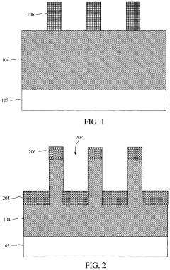
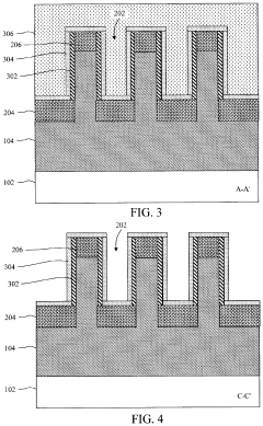
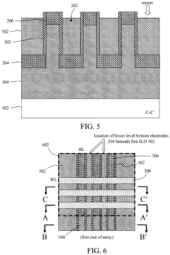
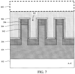
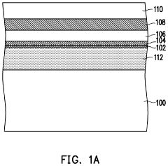
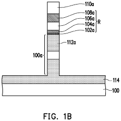
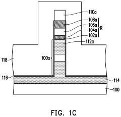
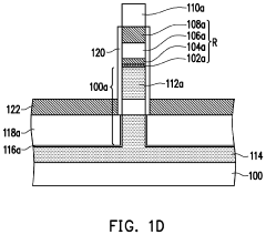
Techniques for Forming RRAM Cells
PatentActiveUS20200243767A1
Innovation
- The method involves forming bottom electrodes at two different levels within the same footprint area, with an insulating layer and top electrodes, where the bottom electrodes include bit lines orthogonal to the word lines, allowing for the creation of an array of RRAM cells with increased density without expanding the device footprint.
Resistive random access memory and manufacturing method thereof
PatentActiveUS11818966B2
Innovation
- Integration of the transistor and resistive random access memory structure in a pillar protruding from the substrate, with a gate dielectric layer, electrodes, doped regions, and a metal silicide layer, allowing for a nanowire transistor electrically connected to the memory structure, enhancing cell density and simplifying manufacturing.
Materials Science Innovations for RRAM Optimization
Materials science innovations represent a critical frontier in advancing RRAM (Resistive Random Access Memory) technology toward higher data density capabilities. The fundamental performance of RRAM devices is largely determined by the properties of the switching materials employed in their construction. Recent research has focused on developing novel material compositions that can support multi-level cell operations while maintaining reliability and endurance.
Metal oxides remain the predominant material class for RRAM applications, with significant advancements in hafnium oxide (HfOx), tantalum oxide (TaOx), and titanium oxide (TiOx) based devices. These materials exhibit favorable switching characteristics, but researchers have begun exploring composite structures and doping strategies to enhance their performance. For instance, introducing dopants such as aluminum or silicon into HfOx has demonstrated improved retention and reduced variability in resistance states.
Layered heterostructures represent another promising direction, where alternating thin films of different materials create engineered interfaces that can precisely control ion migration pathways. These structures have shown potential for achieving more distinct resistance states, directly contributing to increased data density through multi-bit storage capabilities. Recent experiments with HfOx/TaOx bilayers have demonstrated up to 8 distinguishable resistance states in a single memory cell.
Two-dimensional materials, including graphene, MoS2, and hexagonal boron nitride (h-BN), are emerging as intriguing candidates for next-generation RRAM. Their atomically thin nature provides unique electronic properties and potential for extreme scaling. Particularly, h-BN has shown promise as an ultrathin insulating layer that can facilitate controlled filament formation while maintaining excellent thermal stability.
Interface engineering has become increasingly important, with researchers focusing on the electrode-oxide interface where the switching phenomenon primarily occurs. Noble metals like platinum and gold have traditionally been used, but more recent work explores reactive metals and alloys that can form favorable interfacial layers to enhance switching uniformity and reduce operating voltages.
Atomic layer deposition (ALD) and other precision fabrication techniques have enabled unprecedented control over material composition and structure at the nanoscale. This has allowed researchers to create designer materials with tailored defect concentrations and oxygen vacancy distributions—critical factors that determine switching behavior in oxide-based RRAM.
The integration of these material innovations with advanced fabrication techniques presents a clear pathway toward RRAM devices with significantly higher data density, potentially enabling storage capacities that rival or exceed current flash memory while maintaining RRAM's inherent advantages in speed, power consumption, and endurance.
Energy Efficiency Considerations in High-Density RRAM
Energy efficiency has emerged as a critical factor in the development and deployment of high-density RRAM (Resistive Random Access Memory) technologies. As data density increases, power consumption becomes a significant constraint that must be carefully managed to ensure practical implementation in various applications, particularly in mobile and IoT devices where battery life is paramount.
The fundamental energy requirements of RRAM operations stem from the SET and RESET processes that switch the resistance states of memory cells. Current high-density RRAM implementations typically consume between 0.1-10 pJ per bit operation, which becomes substantial when scaled to gigabit or terabit capacities. Research indicates that optimizing the switching material composition can significantly reduce this energy footprint, with hafnium oxide and tantalum oxide showing promising characteristics for low-power operation.
Pulse engineering represents another crucial approach to energy optimization. By carefully tailoring the amplitude, duration, and shape of programming pulses, energy consumption can be reduced by up to 60% compared to conventional square pulses. Particularly, triangular and trapezoidal waveforms have demonstrated enhanced energy efficiency while maintaining reliable switching behavior.
Architectural innovations also contribute substantially to energy efficiency. The crossbar array structure, while optimal for density, introduces sneak path currents that waste energy. Implementing selector devices with high nonlinearity (>10^4) can effectively suppress these parasitic currents. Additionally, hierarchical memory organizations that incorporate caching mechanisms can reduce the frequency of high-energy write operations to the RRAM array.
Voltage scaling techniques offer another avenue for energy optimization. Operating RRAM cells at reduced voltages close to their threshold values can dramatically decrease power consumption, though this approach requires precise control circuitry to maintain reliability. Recent advancements in adaptive voltage scaling algorithms have shown the potential to reduce energy consumption by up to 40% while maintaining acceptable bit error rates.
The relationship between data density and energy efficiency presents interesting trade-offs. While multi-level cell (MLC) approaches increase data density by storing multiple bits per cell, they typically require more precise and energy-intensive programming operations. Research suggests that optimizing for 2-3 bits per cell may represent the sweet spot for energy-efficient high-density storage, beyond which diminishing returns in density are outweighed by exponential increases in energy requirements.
Emerging techniques such as neuromorphic computing approaches that leverage the inherent analog nature of RRAM devices show promise for further energy optimization, potentially reducing energy consumption by orders of magnitude for specific computational tasks while maintaining high data density.
Unlock deeper insights with Patsnap Eureka Quick Research — get a full tech report to explore trends and direct your research. Try now!
Generate Your Research Report Instantly with AI Agent
Supercharge your innovation with Patsnap Eureka AI Agent Platform!