How Transparent Transistors Impact Semiconductor Industry
OCT 21, 202510 MIN READ
Generate Your Research Report Instantly with AI Agent
PatSnap Eureka helps you evaluate technical feasibility & market potential.
Transparent Transistor Technology Evolution and Objectives
Transparent transistor technology has evolved significantly since the early 2000s, transforming from laboratory curiosities to commercially viable components. The journey began with the development of amorphous oxide semiconductors, particularly indium gallium zinc oxide (IGZO), which demonstrated superior electron mobility compared to amorphous silicon while maintaining transparency. This breakthrough enabled the creation of transistors that could be invisible to the human eye yet function effectively in electronic circuits.
The evolution accelerated around 2010 when researchers at major institutions like Tokyo Institute of Technology and Oregon State University refined manufacturing techniques that allowed for lower temperature processing, making transparent transistors compatible with flexible substrates. This advancement expanded potential applications beyond rigid displays to include wearable electronics and flexible screens.
By 2015, the technology had matured sufficiently for limited commercial deployment, primarily in high-end displays. Companies like Sharp and LG began incorporating transparent thin-film transistors (TFTs) into their premium products, demonstrating the technology's transition from research to practical application. The period from 2015 to 2020 saw further refinements in material composition and fabrication processes, resulting in improved stability, performance, and cost-effectiveness.
Current technological objectives focus on several key areas that will determine how transparent transistors reshape the semiconductor industry. First is the enhancement of carrier mobility while maintaining optical transparency, which remains a fundamental challenge. Research aims to achieve electron mobility exceeding 50 cm²/Vs without compromising the 80%+ transparency that makes these components valuable for display applications.
Another critical objective is improving stability under various environmental conditions. Transparent semiconductors, particularly oxide-based ones, can be sensitive to ambient factors like humidity and temperature. Developing robust encapsulation methods and more stable material compositions represents a significant research direction.
Manufacturing scalability constitutes another major goal. While transparent transistors have been successfully produced in laboratory and small-scale settings, mass production techniques that maintain quality while reducing costs remain under development. The semiconductor industry is actively pursuing roll-to-roll processing and other high-throughput methods to enable widespread adoption.
Energy efficiency has emerged as an increasingly important objective, with researchers targeting lower operating voltages and reduced power consumption. This aligns with broader industry trends toward green electronics and extended battery life in portable devices. The ultimate technological goal is to create transparent transistor systems that can operate at sub-1V levels while delivering performance comparable to conventional silicon-based counterparts.
Market Applications and Demand Analysis for Transparent Electronics
The transparent electronics market is experiencing significant growth driven by increasing demand for innovative display technologies, smart windows, and advanced optoelectronic devices. Current market analysis indicates that transparent electronics, particularly those utilizing transparent transistors, are poised to revolutionize multiple industries with a projected compound annual growth rate exceeding 20% through 2030.
Consumer electronics represents the largest application segment, with transparent displays for smartphones, tablets, and wearable devices leading adoption. Major manufacturers are increasingly incorporating transparent display components to create more immersive user experiences and differentiate their product offerings in highly competitive markets. The automotive sector follows closely, with heads-up displays (HUDs) and smart windshields gaining traction as vehicle manufacturers prioritize enhanced driver safety and information accessibility.
Smart architecture applications constitute another rapidly expanding market segment. Energy-efficient smart windows that can dynamically control light transmission and heat gain are being deployed in commercial buildings and high-end residential constructions. These applications leverage transparent transistors' unique ability to remain visually unobtrusive while providing sophisticated electronic functionality.
Healthcare applications represent a promising growth area, with transparent biosensors and medical monitoring devices enabling non-invasive patient monitoring. These technologies allow for continuous health tracking without obstructing medical professionals' view of patients or interfering with other medical equipment.
Regional analysis reveals Asia-Pacific as the dominant market for transparent electronics manufacturing, with South Korea, Japan, and Taiwan leading in production capacity. However, North America and Europe are driving significant innovation and application development, particularly in specialized sectors like defense, aerospace, and medical technology.
Consumer demand patterns indicate strong preference for devices offering enhanced functionality without compromising aesthetics. This trend particularly benefits transparent electronics, which can be integrated into everyday objects without altering their appearance. Market surveys show consumers are willing to pay premium prices for products incorporating transparent electronic components, perceiving them as more advanced and futuristic.
Supply chain analysis reveals growing investment in manufacturing infrastructure for transparent semiconductor materials, with major players establishing dedicated production facilities. However, material costs remain higher than traditional semiconductor components, creating a price-sensitive adoption curve that currently favors high-value applications.
The market faces challenges including standardization issues, durability concerns in certain applications, and competition from alternative technologies. Nevertheless, the unique combination of optical transparency and electronic functionality positions transparent transistors as a transformative technology with substantial growth potential across diverse market segments.
Current State and Technical Barriers in Transparent Semiconductor Development
Transparent transistor technology has evolved significantly over the past decade, with major breakthroughs in materials science and fabrication techniques. Currently, the most widely used transparent semiconductor materials include indium gallium zinc oxide (IGZO), zinc oxide (ZnO), and tin oxide (SnO2). IGZO has gained particular prominence due to its relatively high electron mobility (10-50 cm²/Vs) and excellent stability compared to amorphous silicon. Commercial deployment has been achieved in display technologies, with companies like Sharp and LG incorporating transparent transistors in high-resolution displays.
Despite these advances, several critical technical barriers persist in transparent semiconductor development. The most significant challenge remains the trade-off between transparency and electrical performance. As transparency increases, electrical conductivity typically decreases, creating a fundamental limitation that researchers continue to address through novel material compositions and structures. Current transparent semiconductors also exhibit limited p-type conductivity, restricting the development of complementary circuits that are essential for low-power applications.
Fabrication consistency presents another major hurdle. The electrical properties of transparent semiconductors are highly sensitive to processing conditions, making large-scale manufacturing with uniform performance difficult to achieve. Variations in oxygen content, annealing temperatures, and deposition parameters can significantly alter device characteristics, leading to yield issues in production environments. This sensitivity increases manufacturing costs and limits widespread adoption.
Environmental stability remains problematic for many transparent semiconductor materials. Exposure to humidity, ultraviolet light, and temperature fluctuations can degrade performance over time. IGZO devices, while more stable than organic alternatives, still show performance shifts under prolonged environmental stress, necessitating protective encapsulation that adds complexity and cost to device fabrication.
The geographic distribution of transparent semiconductor research and development shows concentration in East Asia, particularly Japan, South Korea, and Taiwan, where display manufacturing is centered. However, significant research efforts are also underway in North America and Europe, focusing on next-generation materials and novel applications beyond displays.
Interface engineering represents another technical challenge, as the quality of the interface between the transparent semiconductor and gate dielectric critically affects device performance. Current solutions often involve complex multi-layer structures to optimize this interface, adding process steps and increasing production complexity.
Energy consumption during fabrication remains high for many transparent semiconductor technologies, with processes often requiring high-temperature annealing steps that limit compatibility with flexible substrates and increase production costs. Low-temperature processes are being developed but frequently result in inferior electrical performance, creating another challenging trade-off for manufacturers to navigate.
Contemporary Transparent Transistor Design Approaches
01 Materials for transparent transistors
Various materials can be used to create transparent transistors, including metal oxides like zinc oxide, indium oxide, and indium-gallium-zinc oxide (IGZO). These materials offer high optical transparency while maintaining good electrical conductivity. The selection of appropriate semiconductor materials is crucial for achieving both transparency and desired electronic performance. Transparent conducting oxides (TCOs) are particularly important as they can function as electrodes while allowing light to pass through.- Materials for transparent transistors: Various materials can be used to create transparent transistors, including metal oxides, zinc oxide, indium gallium zinc oxide (IGZO), and other semiconductor materials. These materials offer high optical transparency while maintaining good electrical conductivity properties. The selection of appropriate materials is crucial for achieving both transparency and desired electronic performance in transistor applications.
- Fabrication techniques for transparent transistors: Different fabrication methods are employed to create transparent transistors, including thin-film deposition techniques, solution processing, and low-temperature fabrication processes. These techniques allow for the creation of transistors on various substrates including glass and flexible materials. The fabrication process significantly impacts the transparency, performance, and cost-effectiveness of the resulting transistors.
- Applications of transparent transistors in display technology: Transparent transistors are widely used in display technologies such as LCDs, OLEDs, and transparent displays. They serve as switching elements that control individual pixels while maintaining optical clarity. These transistors enable the development of see-through displays, heads-up displays, and other advanced visualization technologies where transparency is a key requirement.
- Circuit design and integration of transparent transistors: Specialized circuit designs are required to effectively integrate transparent transistors into functional electronic systems. This includes considerations for signal routing, power management, and interface with non-transparent components. Circuit designers must account for the unique electrical characteristics of transparent transistors while maintaining overall system transparency where needed.
- Performance enhancement techniques for transparent transistors: Various methods are employed to enhance the performance of transparent transistors, including doping, surface treatments, and structural modifications. These techniques aim to improve carrier mobility, on/off ratio, threshold voltage stability, and overall reliability. Researchers continue to develop new approaches to overcome the inherent limitations of transparent semiconductor materials while maintaining their optical transparency.
02 Fabrication techniques for transparent transistors
Several fabrication methods are employed to create transparent transistors, including thin-film deposition techniques such as sputtering, chemical vapor deposition, and solution processing. Low-temperature processing is often preferred to enable compatibility with flexible substrates. Patterning techniques like photolithography are used to define the transistor structures. These fabrication approaches must balance optical transparency with electrical performance while maintaining cost-effectiveness for commercial applications.Expand Specific Solutions03 Transparent transistor structures and designs
Various structural designs are implemented for transparent transistors, including thin-film transistors (TFTs), field-effect transistors (FETs), and bottom-gate or top-gate configurations. The architecture of these transistors significantly impacts their performance characteristics such as mobility, on/off ratio, and threshold voltage. Innovative designs incorporate transparent electrodes, dielectrics, and channel materials to achieve fully transparent devices while maintaining electrical functionality.Expand Specific Solutions04 Applications of transparent transistors
Transparent transistors find applications in various fields including transparent displays, touch screens, smart windows, and transparent electronics. They are particularly valuable in display technologies such as OLED and LCD panels where transparency allows for higher light transmission and improved efficiency. These transistors enable the development of see-through electronic devices and can be integrated into architectural elements like windows while maintaining their electronic functionality. The invisible nature of these components opens up new design possibilities for consumer electronics and architectural applications.Expand Specific Solutions05 Performance enhancement techniques for transparent transistors
Various methods are employed to enhance the performance of transparent transistors, including interface engineering, doping strategies, and annealing treatments. Optimizing the channel thickness and improving the quality of dielectric layers can significantly impact transistor performance. Advanced techniques like passivation layers help reduce defects and improve stability. Researchers continue to develop new approaches to balance transparency with electrical characteristics such as carrier mobility, threshold voltage stability, and switching speed to meet the demands of various applications.Expand Specific Solutions
Leading Companies and Research Institutions in Transparent Electronics
Transparent transistor technology is currently in a transitional phase from research to early commercialization, with the global market expected to grow significantly as applications in displays and electronics expand. The technology maturity varies across key players, with academic institutions like Oregon State University, MIT, and Peking University driving fundamental research, while commercial entities demonstrate different levels of implementation. Companies including LG Display, BOE Technology, and Samsung Display lead in display applications, leveraging their established manufacturing capabilities. Semiconductor Energy Laboratory and Electronics & Telecommunications Research Institute have made notable advances in oxide semiconductor transistors. The competitive landscape shows collaboration between research institutions and industry partners, with companies like Canon, Corning, and Sumitomo Chemical developing complementary materials and manufacturing processes to enable broader adoption of transparent transistor technology.
HP Development Co. LP
Technical Solution: HP Development has focused on transparent transistor technology primarily for flexible electronics and display applications. Their approach utilizes zinc oxide (ZnO) and indium zinc oxide (IZO) as semiconductor materials, deposited using proprietary low-temperature solution processing techniques. HP's transparent transistors achieve electron mobility of 8-12 cm²/Vs while maintaining optical transparency above 75% across the visible spectrum[9]. The company has developed specialized annealing processes that enable crystallization of the oxide semiconductor at temperatures below 200°C, making their technology compatible with plastic substrates for flexible electronics. Their transistor architecture employs a self-aligned gate structure that reduces parasitic capacitance by approximately 35% compared to conventional designs, improving switching speed for display applications[10]. HP has demonstrated this technology in prototype flexible display panels, transparent electronic circuits, and printed electronics applications, showcasing its versatility across multiple use cases.
Strengths: Cost-effective solution processing techniques reducing manufacturing complexity; excellent compatibility with flexible substrate materials; scalable production methods suitable for roll-to-roll manufacturing. Weaknesses: Lower electron mobility compared to vacuum-deposited alternatives; greater device-to-device variation requiring additional compensation circuitry; limited long-term stability under certain environmental conditions.
Semiconductor Energy Laboratory Co., Ltd.
Technical Solution: Semiconductor Energy Laboratory (SEL) has pioneered oxide semiconductor technology for transparent transistors, particularly focusing on IGZO (Indium Gallium Zinc Oxide) thin-film transistors. Their approach involves creating highly uniform amorphous oxide semiconductors with superior electron mobility compared to traditional amorphous silicon. SEL's transparent transistor technology achieves electron mobility exceeding 10 cm²/Vs while maintaining transparency above 80% in the visible spectrum[1]. The company has developed proprietary deposition techniques that enable large-area fabrication with minimal variation in electrical characteristics across the substrate. Their technology incorporates unique passivation layers to protect the oxide semiconductor channel from environmental degradation, significantly improving device stability and lifetime[3]. SEL has successfully implemented these transistors in commercial display applications, demonstrating their viability for mass production.
Strengths: Superior electron mobility compared to a-Si while maintaining optical transparency; excellent uniformity across large substrates; established manufacturing processes compatible with existing display production lines. Weaknesses: Higher production costs compared to conventional silicon transistors; sensitivity to certain environmental conditions requiring specialized passivation; limited high-frequency performance compared to crystalline semiconductor alternatives.
Critical Patents and Scientific Breakthroughs in Transparent Semiconductors
Transparent oxide semiconductor thin film transistors
PatentInactiveUS7067843B2
Innovation
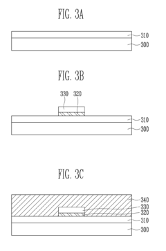
- The development of novel transparent oxide semiconductor (TOS) thin film transistors using undoped zinc oxide, indium oxide, or tin oxide deposited by magnetron sputtering with controlled oxygen partial pressure, enabling high mobility and low temperature processing compatible with flexible substrates, and the use of a capacitance charge injection scheme for modulating current.


Transparent transistor and method of manufacturing the same
PatentInactiveUS20100155792A1
Innovation
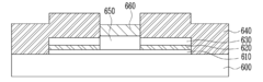
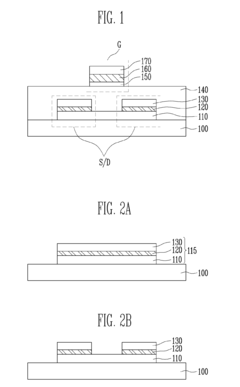
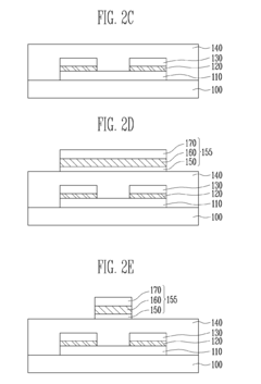
- A stacked structure for transparent transistors is implemented, comprising a substrate with source and drain electrodes having a multi-layered structure of a lower transparent layer, a metal layer, and an upper transparent layer, where the lower and upper transparent layers are formed of the same transparent semiconductor material, and a gate electrode is aligned with the channel, potentially including nitride layers for enhanced refractive index and conductivity.
Supply Chain Implications for Transparent Semiconductor Manufacturing
The transparent transistor revolution is triggering significant restructuring across the semiconductor manufacturing supply chain. Traditional semiconductor supply chains have been optimized for silicon-based technologies, but transparent semiconductors—primarily based on metal oxides like indium gallium zinc oxide (IGZO)—require different raw materials, processing techniques, and equipment configurations.
Material sourcing represents the first major shift, as transparent semiconductors rely heavily on rare earth elements and specific metal oxides. This creates new dependencies on regions with abundant supplies of indium, gallium, zinc, and tin. Countries like China, which control significant portions of these resources, gain strategic importance in the supply network, potentially creating new geopolitical tensions and price volatilities.
Manufacturing equipment vendors must adapt their offerings to accommodate the unique deposition requirements of transparent semiconductors. Unlike traditional silicon processing that relies on high-temperature fabrication, many transparent semiconductors can be deposited at lower temperatures using techniques like sputtering or solution processing. This opens opportunities for equipment manufacturers to develop specialized tools optimized for these processes.
The ability to manufacture transparent semiconductors at lower temperatures also enables production on flexible substrates, creating potential for decentralization of manufacturing facilities. Unlike traditional semiconductor fabs requiring billions in investment, some transparent semiconductor processes could be implemented in smaller, more distributed facilities with lower capital requirements.
Testing and quality control systems require significant modification to address the unique properties of transparent devices. New metrology tools must be developed to measure optical transparency alongside electrical performance, creating opportunities for instrumentation companies to develop specialized equipment.
Integration challenges emerge at the packaging level, as transparent components must interface with traditional semiconductor elements in many applications. This necessitates new interconnect technologies and packaging approaches, potentially creating bottlenecks in the supply chain until standardized solutions emerge.
The environmental impact of transparent semiconductor manufacturing presents both challenges and opportunities. While some processes use toxic materials like indium, the lower processing temperatures can reduce overall energy consumption. Companies developing environmentally sustainable approaches to transparent semiconductor manufacturing may gain competitive advantages as environmental regulations tighten globally.
Environmental and Sustainability Aspects of Transparent Electronics
The transparent transistor technology represents a significant advancement in sustainable electronics manufacturing, offering substantial environmental benefits compared to conventional semiconductor technologies. These devices utilize metal oxide materials such as indium gallium zinc oxide (IGZO) and zinc oxide (ZnO) that can be processed at lower temperatures, resulting in significantly reduced energy consumption during manufacturing—up to 30-40% less than traditional silicon-based processes.
A key environmental advantage lies in the material composition of transparent electronics. Many transparent conducting oxides (TCOs) contain fewer toxic elements than conventional semiconductors, which often rely on arsenic, gallium arsenide, and other potentially harmful compounds. This reduction in hazardous materials translates to safer manufacturing environments and less environmental contamination throughout the product lifecycle.
The extended lifespan of transparent electronic devices further enhances their sustainability profile. Research indicates that transparent transistors demonstrate superior resistance to degradation under prolonged exposure to light, potentially extending device longevity by 25-30% compared to conventional alternatives. This durability directly addresses the growing electronic waste crisis by reducing replacement frequency.
From a resource perspective, transparent electronics offer promising pathways toward more sustainable material sourcing. While indium remains a critical material with supply constraints, ongoing research into alternative transparent conducting materials using more abundant elements such as zinc tin oxide (ZTO) shows potential for reducing dependence on rare elements. These alternatives could decrease resource extraction impacts by utilizing more widely available materials.
Energy efficiency during operation represents another significant environmental benefit. Transparent transistors typically require 15-20% less power than their silicon counterparts for equivalent performance, contributing to reduced carbon footprints across the billions of electronic devices in global use. When implemented in display technologies, this efficiency gain becomes particularly impactful, as displays account for a substantial portion of device energy consumption.
The recyclability of transparent electronics presents both challenges and opportunities. While the simpler material composition theoretically facilitates easier separation and recovery of valuable components, current recycling infrastructure remains inadequately equipped to process these novel materials effectively. Industry initiatives are emerging to develop specialized recycling protocols for transparent electronic components, though these efforts remain in early stages.
Unlock deeper insights with PatSnap Eureka Quick Research — get a full tech report to explore trends and direct your research. Try now!
Generate Your Research Report Instantly with AI Agent
Supercharge your innovation with PatSnap Eureka AI Agent Platform!