How Transparent Transistors Improve High-Frequency Devices
OCT 21, 202510 MIN READ
Generate Your Research Report Instantly with AI Agent
PatSnap Eureka helps you evaluate technical feasibility & market potential.
Transparent Transistor Technology Evolution and Objectives
Transparent transistor technology has evolved significantly since the early 2000s, transforming from laboratory curiosities to essential components in modern high-frequency electronic devices. The journey began with the development of amorphous oxide semiconductors, particularly indium gallium zinc oxide (IGZO), which demonstrated unprecedented combinations of optical transparency and electron mobility. This breakthrough enabled the creation of transistors that could operate at higher frequencies while remaining visually transparent, opening new possibilities for integrated electronics in displays and communication systems.
The evolution of transparent transistor technology has been driven by several key factors, including the demand for higher bandwidth in wireless communications, the need for more sophisticated display technologies, and the growing interest in transparent electronics for augmented reality applications. Each advancement has pushed the boundaries of material science and semiconductor physics, leading to continuous improvements in performance metrics such as carrier mobility, on/off ratio, and frequency response.
A significant milestone in this evolution was the transition from silicon-based to oxide-based semiconductors. While silicon dominated traditional electronics, its opaque nature limited applications requiring transparency. The emergence of wide-bandgap oxide semiconductors provided a solution, offering both transparency to visible light and suitable electronic properties for high-frequency operation. This shift represented not just a material change but a fundamental rethinking of transistor design principles.
Recent years have witnessed the refinement of fabrication techniques, enabling the production of transparent transistors with nanoscale dimensions. These advancements have dramatically improved switching speeds and reduced parasitic capacitances, critical factors for high-frequency performance. Additionally, innovations in electrode materials and device architectures have enhanced the integration capabilities of transparent transistors with conventional electronics, facilitating their adoption in commercial applications.
The primary objective of transparent transistor technology development is to achieve a perfect balance between optical transparency and electronic performance. Researchers aim to create devices that maintain at least 80% transparency across the visible spectrum while delivering switching frequencies in the gigahertz range. This goal requires overcoming fundamental material limitations and developing novel fabrication approaches that preserve both optical and electronic properties.
Another crucial objective is the enhancement of reliability and stability under various operating conditions. High-frequency applications often involve elevated temperatures and electrical stresses, which can degrade transparent semiconductor materials over time. Addressing these challenges requires comprehensive understanding of degradation mechanisms and the development of protective strategies to ensure long-term performance consistency.
Looking forward, the technology roadmap for transparent transistors includes objectives related to flexibility, energy efficiency, and integration density. As applications expand into wearable electronics and Internet of Things (IoT) devices, transparent transistors must evolve to accommodate mechanical deformation while maintaining their high-frequency capabilities. This evolution represents the next frontier in transparent electronics, promising to revolutionize how we interact with technology in our daily lives.
Market Applications for High-Frequency Transparent Electronics
The transparent transistor technology is revolutionizing high-frequency electronics across multiple market sectors. In consumer electronics, transparent high-frequency devices are enabling next-generation smartphones and wearable technology with improved signal processing capabilities while maintaining aesthetic appeal. These devices can integrate seamlessly into smart glasses, windshields, and display panels, creating interactive surfaces that maintain transparency while delivering high-performance computing and communication functions.
The automotive industry represents another significant market opportunity, with transparent high-frequency electronics being incorporated into heads-up displays (HUDs) and advanced driver-assistance systems (ADAS). These applications benefit from the combination of optical transparency and high-frequency operation, allowing for real-time data processing and display without obstructing the driver's view. The technology enables enhanced radar and sensor systems that can be integrated directly into windshields and windows.
In healthcare, transparent high-frequency devices are finding applications in medical imaging equipment and patient monitoring systems. The ability to process high-frequency signals while maintaining visibility through the device allows for innovative diagnostic tools and non-invasive monitoring solutions. Medical wearables utilizing this technology can provide continuous health monitoring while remaining virtually invisible on the patient's body.
The telecommunications sector stands to benefit substantially from transparent high-frequency electronics. Next-generation 5G and future 6G infrastructure can utilize transparent antennas and signal processing components that can be integrated into building materials, windows, and urban infrastructure without visual disruption. This enables denser network deployment in urban environments without aesthetic compromise.
Military and aerospace applications represent a premium market segment for transparent high-frequency electronics. These include advanced radar systems, communication equipment, and heads-up displays for aircraft and combat vehicles. The combination of transparency and high-frequency operation allows for equipment that can be integrated into cockpit canopies and vehicle windows without compromising visibility or performance.
The Internet of Things (IoT) market presents perhaps the broadest application potential, with transparent high-frequency devices enabling smart home technologies, industrial sensors, and environmental monitoring systems that can be deployed unobtrusively. These devices can be integrated into windows, appliances, and building materials, creating truly ambient intelligence without visual clutter.
Current Limitations and Technical Challenges in Transparent Transistors
Despite the promising advancements in transparent transistor technology, several significant limitations and technical challenges persist that hinder their widespread implementation in high-frequency applications. The primary constraint remains the inherently lower carrier mobility in transparent semiconducting materials compared to conventional silicon-based semiconductors. While silicon can achieve electron mobility exceeding 1,000 cm²/Vs, most transparent oxide semiconductors struggle to surpass 100 cm²/Vs under optimal conditions, with typical commercial implementations achieving only 10-40 cm²/Vs.
Channel resistance issues present another critical challenge, as the resistance in transparent transistors is generally higher than in silicon counterparts, leading to increased power consumption and heat generation during high-frequency operation. This becomes particularly problematic when scaling down device dimensions for improved performance, as the resistance increases disproportionately at smaller scales.
Stability under operational stress represents a significant hurdle for transparent transistors in high-frequency applications. When subjected to continuous high-frequency switching, many transparent semiconductor materials exhibit threshold voltage shifts and performance degradation over time. This instability is often attributed to charge trapping at the semiconductor-dielectric interface and oxygen vacancy migration within the semiconductor layer.
Manufacturing consistency poses substantial challenges as well. Current fabrication processes for transparent transistors suffer from batch-to-batch variations that affect electrical characteristics. The sensitivity of oxide semiconductors to processing conditions, particularly oxygen partial pressure during deposition, makes it difficult to achieve uniform performance across large substrates or between production runs.
Interface quality between the various layers in transparent transistors significantly impacts high-frequency performance. Poor interfaces lead to increased carrier scattering and trap states, which degrade frequency response. The development of compatible dielectric materials that form high-quality interfaces with transparent semiconductors remains an active research area.
Parasitic capacitance effects become increasingly dominant at higher frequencies, limiting the maximum operating frequency of transparent transistors. Current device architectures have not been fully optimized to minimize these parasitic elements, resulting in performance limitations above certain frequency thresholds, typically in the low GHz range.
Temperature sensitivity presents another challenge, as most transparent semiconductor materials exhibit significant changes in electrical properties with temperature variations. This thermal instability complicates their use in high-frequency applications where consistent performance across operating temperatures is essential.
Finally, integration challenges with existing electronic systems remain substantial. The different processing requirements, voltage levels, and signal characteristics of transparent transistors compared to conventional silicon electronics create compatibility issues that must be addressed before widespread adoption in high-frequency applications can occur.
State-of-the-Art Transparent Transistor Architectures
01 Transparent oxide semiconductor materials for high-frequency transistors
Transparent oxide semiconductors such as zinc oxide, indium oxide, and indium-gallium-zinc oxide (IGZO) are used to create transparent transistors capable of high-frequency operation. These materials combine optical transparency with good electron mobility, making them suitable for applications requiring both transparency and high-frequency performance. The unique band structure of these oxides allows for efficient carrier transport while maintaining transparency in the visible spectrum.- Transparent oxide semiconductor materials for high-frequency transistors: Transparent oxide semiconductors such as zinc oxide (ZnO), indium gallium zinc oxide (IGZO), and indium tin oxide (ITO) are used to create transparent transistors capable of high-frequency operation. These materials combine optical transparency with good electron mobility, making them suitable for applications requiring both visibility and high-speed performance. The crystalline structure and composition of these oxides can be optimized to enhance carrier mobility and frequency response while maintaining transparency.
- High-frequency circuit design for transparent transistor applications: Specialized circuit designs are implemented to optimize the high-frequency performance of transparent transistors. These designs include impedance matching networks, feedback mechanisms, and advanced biasing techniques that compensate for the inherent limitations of transparent semiconductor materials. By carefully engineering the circuit topology and component values, the frequency response and gain of transparent transistor circuits can be significantly improved, enabling their use in radio frequency (RF) and microwave applications.
- Fabrication techniques for transparent high-frequency transistors: Advanced fabrication methods are employed to create transparent transistors with enhanced high-frequency capabilities. These techniques include low-temperature deposition processes, precise patterning methods, and specialized annealing treatments that optimize the interface between different layers. The channel length is minimized while maintaining structural integrity to reduce parasitic capacitances and increase the cut-off frequency. Additionally, novel gate structures are implemented to improve electrostatic control and frequency response.
- Integration of transparent transistors in high-frequency communication systems: Transparent transistors are integrated into high-frequency communication systems where optical transparency provides unique advantages. These applications include transparent antennas, see-through displays with integrated RF circuits, and optically transparent wireless communication modules. The integration requires specialized packaging techniques and interconnect solutions that maintain both the optical and electrical properties of the devices. This approach enables new form factors for communication equipment and enhances functionality in space-constrained applications.
- Performance enhancement techniques for transparent high-frequency transistors: Various methods are employed to enhance the high-frequency performance of transparent transistors. These include doping optimization to increase carrier concentration, interface engineering to reduce scattering, and the use of novel dielectric materials to improve gate capacitance characteristics. Additionally, strain engineering and heterostructure designs are implemented to boost carrier mobility. These enhancements collectively improve the transistor's gain, noise figure, and maximum oscillation frequency while maintaining optical transparency.
02 High-frequency circuit design for transparent transistor applications
Specialized circuit designs are implemented to optimize the high-frequency performance of transparent transistors. These designs include impedance matching networks, feedback mechanisms, and advanced biasing techniques that compensate for the inherent limitations of transparent semiconductor materials. By carefully engineering the circuit topology, the frequency response of transparent transistors can be extended to meet the requirements of high-frequency applications while maintaining optical transparency.Expand Specific Solutions03 Fabrication techniques for transparent high-frequency transistors
Advanced fabrication methods are employed to create transparent transistors with high-frequency capabilities. These techniques include low-temperature deposition processes, precise patterning methods, and specialized annealing procedures that optimize the crystalline structure of transparent semiconductors. The fabrication approaches focus on minimizing defects and interface states that could degrade high-frequency performance while preserving the optical transparency of the devices.Expand Specific Solutions04 Integration of transparent transistors in high-frequency systems
Transparent high-frequency transistors are integrated into various electronic systems that benefit from optical transparency. These include transparent displays with integrated drivers, see-through radio frequency identification (RFID) tags, and transparent antennas with active components. The integration approaches address challenges related to connecting transparent components with conventional electronics while maintaining system-level high-frequency performance and optical clarity.Expand Specific Solutions05 Performance enhancement techniques for transparent high-frequency transistors
Various methods are employed to enhance the high-frequency performance of transparent transistors. These include channel engineering, gate dielectric optimization, and contact resistance reduction techniques. Advanced doping strategies and heterostructure designs are also utilized to improve carrier mobility and reduce parasitic capacitances, resulting in higher cutoff frequencies while maintaining optical transparency. These enhancements enable transparent transistors to operate effectively in high-frequency applications.Expand Specific Solutions
Leading Companies and Research Institutions in Transparent Electronics
Transparent transistor technology is currently in a growth phase, with increasing market adoption driven by high-frequency device applications. The market is expanding rapidly as companies like Samsung Display, LG Display, and Japan Display invest heavily in research and development. Technical maturity varies across players, with academic institutions like Oregon State University and Northwestern University establishing fundamental research, while commercial entities including Taiwan Semiconductor Manufacturing Co., Semiconductor Energy Laboratory, and Sharp Corp. are advancing practical implementations. Companies such as NXP Semiconductors and Qualcomm are exploring high-frequency applications, while display manufacturers are integrating transparent transistors into next-generation products. The technology shows promising convergence between semiconductor and display industries, with significant potential for growth in mobile, automotive, and IoT applications.
LG Display Co., Ltd.
Technical Solution: LG Display has developed a comprehensive transparent transistor technology platform focused on metal oxide semiconductors, particularly IGZO (Indium Gallium Zinc Oxide) and ZnO-based materials. Their approach integrates these transparent semiconductors with specialized transparent electrodes made from materials like ITO (Indium Tin Oxide) and novel transparent conductive oxides. LG's manufacturing process employs low-temperature deposition techniques (below 300°C) that enable fabrication on various substrates including flexible polymers. Their transistors achieve transparency levels exceeding 85% across the visible spectrum while maintaining electron mobility of 15-20 cm²/Vs. For high-frequency applications, LG has implemented self-aligned gate structures that minimize overlap capacitance, reducing RC delays and enabling switching frequencies up to 10MHz. This technology has been successfully integrated into their transparent display products, enabling faster refresh rates and improved touch response while maintaining visual transparency. LG has also developed specialized passivation layers that enhance device stability under various environmental conditions while preserving transparency.
Strengths: Vertical integration capabilities from materials to finished products; extensive manufacturing infrastructure for large-scale production; strong intellectual property portfolio in transparent electronics. Weaknesses: Relatively higher cost structure compared to conventional technologies; challenges in achieving uniform electrical characteristics across large areas; performance limitations in extreme environmental conditions.
Semiconductor Energy Laboratory Co., Ltd.
Technical Solution: Semiconductor Energy Laboratory (SEL) has pioneered advanced oxide semiconductor technology for transparent transistors, particularly focusing on IGZO (Indium Gallium Zinc Oxide) materials. Their approach involves creating highly uniform amorphous oxide semiconductors with carefully controlled oxygen vacancy concentrations to achieve optimal carrier mobility. SEL has developed proprietary deposition techniques that enable the creation of ultra-thin, highly transparent active layers with thickness below 50nm while maintaining excellent electrical characteristics. Their transistors demonstrate electron mobility exceeding 10 cm²/Vs, significantly higher than conventional amorphous silicon, while maintaining transparency above 80% in the visible spectrum. For high-frequency applications, SEL has implemented specialized gate structures with reduced parasitic capacitance and optimized channel lengths below 5μm, enabling operation frequencies in the MHz range while maintaining transparency. This technology has been successfully integrated into various display products requiring high refresh rates and fast response times.
Strengths: Industry-leading expertise in oxide semiconductor materials with exceptional carrier mobility-transparency balance; established manufacturing processes suitable for large-area electronics; proven track record of commercial implementation. Weaknesses: Higher production costs compared to conventional silicon technologies; potential long-term stability issues under certain environmental conditions; limited performance in extremely high-frequency applications compared to crystalline semiconductors.
Key Patents and Scientific Breakthroughs in Transparent Semiconductors
Transparent transistor and method of manufacturing the same
PatentInactiveUS20100155792A1
Innovation
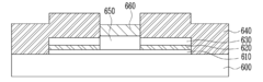
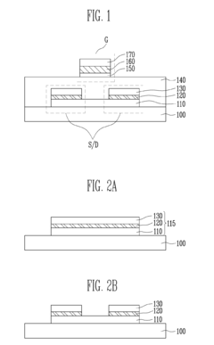
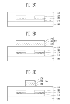
- A stacked structure for transparent transistors is implemented, comprising a substrate with source and drain electrodes having a multi-layered structure of a lower transparent layer, a metal layer, and an upper transparent layer, where the lower and upper transparent layers are formed of the same transparent semiconductor material, and a gate electrode is aligned with the channel, potentially including nitride layers for enhanced refractive index and conductivity.
Transistor structures and methods for making the same
PatentInactiveUS20080108198A1
Innovation
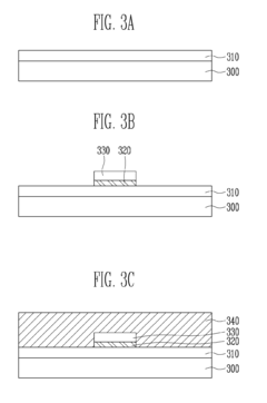
- Development of enhancement-mode, field-effect transistors with a substantially transparent channel layer made from materials like ZnO, SnO2, or In2O3, which are produced by annealing and include a gate insulator layer, source, and drain, allowing for electron accumulation and extraction at the channel layer/gate insulator interface, enabling high optical transmission and efficient electron flow.


Manufacturing Processes and Scalability Considerations
The manufacturing processes for transparent transistors present unique challenges and opportunities that significantly impact their integration into high-frequency devices. Traditional semiconductor fabrication techniques require substantial modification to accommodate the transparent nature of these components. Currently, the most widely adopted manufacturing methods include physical vapor deposition (PVD), chemical vapor deposition (CVD), and solution-based processes such as spin coating and inkjet printing. Each approach offers distinct advantages in terms of film quality, process temperature, and compatibility with flexible substrates.
Physical vapor deposition techniques, particularly sputtering and pulsed laser deposition, enable precise control over film thickness and composition, critical for achieving consistent electrical performance in high-frequency applications. However, these vacuum-based processes face scalability limitations due to equipment costs and throughput constraints. Chemical vapor deposition offers improved uniformity over large areas but typically requires higher processing temperatures that may restrict substrate selection.
Solution-based manufacturing routes have emerged as promising alternatives for large-scale production. These low-temperature processes are compatible with temperature-sensitive substrates and enable roll-to-roll manufacturing capabilities. Recent advancements in precursor chemistry have significantly improved the electrical properties of solution-processed transparent semiconductors, narrowing the performance gap with vacuum-deposited counterparts.
Scalability considerations extend beyond process selection to include yield management and device uniformity across large substrate areas. The industry has witnessed substantial progress in addressing these challenges through innovations in process control and in-line monitoring techniques. Statistical process control methodologies, adapted from conventional semiconductor manufacturing, have been implemented to maintain consistent electrical characteristics across production batches.
Integration with existing manufacturing infrastructure represents another critical factor for commercial viability. Hybrid approaches that combine conventional silicon-based components with transparent transistor elements require careful interface engineering and compatible process sequences. Several leading electronics manufacturers have demonstrated pilot production lines that successfully incorporate transparent transistor fabrication into modified CMOS process flows.
Material supply chain considerations also impact manufacturing scalability. The reliance on indium in many transparent conducting oxides presents potential supply constraints, driving research toward alternative material systems based on more abundant elements. Recent developments in zinc-tin oxide and aluminum-doped zinc oxide systems show promise for addressing these concerns while maintaining the performance requirements for high-frequency applications.
Environmental Impact and Sustainability of Transparent Electronic Materials
The environmental impact of transparent electronic materials, particularly those used in transparent transistors for high-frequency devices, represents a critical consideration in the sustainable development of next-generation electronics. Traditional semiconductor manufacturing processes involve energy-intensive fabrication steps and hazardous chemicals, contributing significantly to environmental degradation. In contrast, many transparent conducting oxides (TCOs) and transparent semiconducting oxides (TSOs) can be fabricated using less resource-intensive methods, such as solution processing at lower temperatures.
Metal oxide-based transparent transistors, especially those utilizing indium gallium zinc oxide (IGZO) and zinc tin oxide (ZTO), demonstrate promising environmental advantages compared to conventional silicon-based technologies. These materials can be deposited using techniques that consume less energy and generate fewer waste byproducts. Additionally, the ability to fabricate these devices on flexible substrates reduces material consumption and enables more efficient use of resources throughout the product lifecycle.
However, sustainability challenges persist in the transparent electronics sector. The reliance on rare elements like indium raises concerns about resource depletion and geopolitical supply risks. Current estimates suggest that indium reserves may face significant pressure as demand for transparent electronics continues to grow. This has prompted research into alternative materials using more abundant elements, such as aluminum-doped zinc oxide (AZO) and fluorine-doped tin oxide (FTO), which could provide more sustainable pathways for high-frequency transparent device development.
The end-of-life management of transparent electronic materials presents both challenges and opportunities. Unlike traditional electronics, many transparent devices can be designed with improved recyclability profiles. Research indicates that up to 60% of the valuable materials in transparent electronic components could potentially be recovered through advanced recycling processes, compared to only 15-20% in conventional electronics. This circular economy approach could significantly reduce the environmental footprint of high-frequency transparent devices.
Energy efficiency during operation represents another environmental advantage of transparent transistors in high-frequency applications. The wide bandgap characteristics of transparent semiconducting materials enable devices to operate at higher frequencies with lower power consumption. Studies demonstrate that transparent high-frequency devices can achieve up to 40% reduction in energy consumption compared to their opaque counterparts, contributing to reduced carbon emissions throughout the product lifecycle.
Looking forward, the integration of biodegradable substrates with transparent electronic materials offers promising directions for truly sustainable high-frequency devices. Recent advances in cellulose-based and other bio-derived substrates compatible with transparent transistor fabrication suggest pathways toward electronics that minimize environmental impact from production through disposal, aligning technological advancement with ecological responsibility.
Unlock deeper insights with PatSnap Eureka Quick Research — get a full tech report to explore trends and direct your research. Try now!
Generate Your Research Report Instantly with AI Agent
Supercharge your innovation with PatSnap Eureka AI Agent Platform!