Materials And Fabrication Methods To Improve Qubit Coherence For QEC
SEP 2, 20259 MIN READ
Generate Your Research Report Instantly with AI Agent
Patsnap Eureka helps you evaluate technical feasibility & market potential.
Quantum Coherence Technology Background and Objectives
Quantum computing has evolved significantly since its theoretical conception in the 1980s, with coherence time emerging as a critical bottleneck for practical quantum error correction (QEC) implementation. The fundamental challenge lies in maintaining quantum states long enough to perform meaningful computations while protecting them from environmental decoherence. Early qubits exhibited coherence times of mere microseconds, severely limiting computational capabilities and making error correction nearly impossible.
The progression of materials science and fabrication techniques has driven substantial improvements in qubit coherence over the past decade. Superconducting qubits, initially limited by material defects and electromagnetic interference, have seen coherence times increase from microseconds to hundreds of microseconds through innovations in substrate purification and circuit design. Similarly, trapped ion systems have achieved coherence times approaching seconds, while topological qubits promise inherent protection against certain error types.
Current technological objectives focus on achieving the coherence thresholds necessary for implementing practical QEC protocols. The primary goal is to develop materials and fabrication methods that can consistently produce qubits with coherence times exceeding the error correction threshold, typically requiring error rates below 1%. This translates to coherence times in the millisecond range for superconducting systems and potentially longer for other qubit modalities.
Beyond mere extension of coherence times, researchers aim to understand and mitigate the fundamental sources of decoherence at the material interface level. This includes addressing two-level system (TLS) defects in amorphous materials, reducing magnetic flux noise, and minimizing the impact of cosmic radiation on superconducting circuits. The development of novel materials with reduced loss tangents and improved fabrication techniques with atomic-level precision represents key objectives in this field.
The ultimate technological goal is to enable fault-tolerant quantum computation through scalable QEC implementation. This requires not only extending coherence times but also developing materials and fabrication methods compatible with large-scale integration. The ability to manufacture thousands to millions of highly coherent qubits with consistent properties represents the horizon challenge for quantum computing hardware development.
Industry roadmaps suggest that achieving practical quantum advantage for complex problems will require coherence improvements of 1-2 orders of magnitude beyond current capabilities. This ambitious target drives research into exotic materials like ultra-high-purity epitaxial superconductors, novel substrate treatments, and three-dimensional integration techniques that minimize crosstalk while maintaining fabrication scalability.
Market Analysis for Quantum Error Correction Solutions
The quantum error correction (QEC) solutions market is experiencing significant growth as quantum computing transitions from research laboratories to commercial applications. Current market estimates value the global quantum computing market at approximately $500 million, with QEC-specific solutions comprising about 15% of this segment. Industry analysts project this market to expand at a compound annual growth rate of 25-30% over the next five years, potentially reaching $2.5 billion by 2028.
Market demand for improved qubit coherence materials and fabrication methods is primarily driven by major quantum computing hardware developers, including IBM, Google, Rigetti, and IonQ. These companies are investing heavily in materials science research to overcome the decoherence challenge that currently limits practical quantum advantage. Government research institutions and national laboratories represent another significant market segment, with countries like the United States, China, and the European Union allocating substantial funding for quantum technology development programs.
The market structure is currently bifurcated between established technology corporations with quantum divisions and specialized quantum startups. Large corporations typically pursue vertical integration strategies, developing proprietary materials and fabrication techniques in-house. In contrast, an emerging ecosystem of specialized materials suppliers and fabrication service providers is forming to support smaller quantum computing companies that lack extensive manufacturing capabilities.
From a geographical perspective, North America dominates the market with approximately 45% share, followed by Europe (30%) and Asia-Pacific (20%). China's national quantum initiative is rapidly accelerating its market position, particularly in materials research for superconducting qubits.
Customer segmentation reveals three primary buyer categories: quantum hardware manufacturers seeking materials improvements, research institutions developing next-generation quantum technologies, and government agencies pursuing strategic quantum capabilities. Each segment has distinct requirements regarding material purity, fabrication precision, and performance metrics.
The pricing structure for advanced materials and fabrication services for quantum applications carries a significant premium, often 5-10 times higher than comparable materials for conventional electronics, reflecting both the specialized nature of these materials and the relatively low production volumes.
Market entry barriers remain substantial due to the highly specialized knowledge required, significant capital investment needs, and the importance of intellectual property protection in this nascent field. Companies with established expertise in ultra-high purity materials processing, cryogenic systems, or precision nanofabrication possess natural advantages when entering this market.
Current Materials Challenges in Qubit Coherence
The pursuit of quantum error correction (QEC) faces significant materials-related obstacles that directly impact qubit coherence times. Current superconducting qubits predominantly utilize aluminum for their Josephson junctions and niobium for resonators, but these materials exhibit inherent limitations. Interface losses at metal-substrate boundaries, particularly between aluminum and silicon or sapphire substrates, introduce decoherence channels that significantly reduce T1 and T2 times.
Surface oxides present another critical challenge, as naturally forming aluminum oxide layers contain paramagnetic impurities and two-level systems (TLS) that couple to the qubit, causing frequency fluctuations and energy dissipation. These TLS are particularly problematic at millikelvin temperatures where quantum processors operate, as they become dominant noise sources.
Material defects within the substrate, including crystal dislocations, impurities, and dangling bonds, contribute substantially to decoherence. Silicon substrates, while offering good compatibility with existing fabrication techniques, contain nuclear spins that interact with qubits. Sapphire substrates reduce this issue but introduce challenges in scaling and integration with control electronics.
Fabrication-induced damage represents another significant hurdle. Current lithographic processes, particularly electron-beam lithography used for precise Josephson junction definition, can introduce charged defects and structural imperfections. Etching processes using reactive ions can damage surfaces and create additional trap states that act as decoherence sources.
The materials challenge extends to interconnects and control lines, where impedance mismatches and parasitic capacitances introduce noise and crosstalk between qubits. Conventional metals used for these components, such as copper and gold, can introduce magnetic impurities that disrupt qubit operation.
Thermal contraction mismatches between different materials in the quantum stack create mechanical stress during cooldown to operating temperatures, potentially altering critical device parameters and introducing additional decoherence channels. This becomes increasingly problematic as system complexity grows.
Achieving the error rates required for practical QEC (below 10^-3) necessitates significant improvements in material purity, interface engineering, and fabrication precision. Current state-of-the-art superconducting qubits achieve coherence times of 100-300 microseconds, whereas practical QEC implementations may require coherence times approaching milliseconds, highlighting the substantial materials engineering challenges that must be overcome.
State-of-the-Art Materials for Enhanced Qubit Coherence
01 Superconducting materials for qubit fabrication
Superconducting materials are widely used in qubit fabrication to enhance coherence times. These materials, when cooled below their critical temperature, exhibit zero electrical resistance and can maintain quantum states for longer periods. Common superconducting materials include aluminum, niobium, and certain alloys that are deposited using techniques such as molecular beam epitaxy or sputtering. The quality of these materials and their interfaces significantly impacts qubit performance by reducing decoherence caused by material defects and impurities.- Superconducting materials for qubit fabrication: Superconducting materials are crucial for fabricating qubits with high coherence times. These materials, when cooled to extremely low temperatures, exhibit quantum mechanical properties that allow for the creation of quantum bits. The fabrication methods involve depositing thin films of superconducting materials like aluminum, niobium, or tantalum on substrates using techniques such as molecular beam epitaxy or sputtering. The quality of these films directly impacts the coherence time of the qubits, with higher purity materials generally yielding better performance.
- Surface treatment and cleaning techniques: Surface treatment and cleaning techniques are essential for improving qubit coherence by reducing noise sources at material interfaces. These techniques include chemical cleaning, ion milling, and plasma treatments to remove contaminants and oxides that can act as sources of decoherence. Advanced methods such as atomic layer etching can be used to create atomically smooth surfaces, which minimize the presence of two-level systems that contribute to decoherence. Proper surface preparation before and during fabrication significantly enhances qubit performance and stability.
- Josephson junction optimization: Josephson junctions are critical components in many qubit designs, particularly in superconducting quantum computing. The fabrication methods for these junctions, including shadow evaporation and double-angle deposition techniques, significantly impact qubit coherence. Controlling the tunnel barrier thickness and uniformity is essential for creating junctions with consistent properties. Advanced techniques like epitaxial growth of junction materials can reduce defects and improve coherence times. The geometry and materials used in junction fabrication directly affect the qubit's susceptibility to noise and decoherence mechanisms.
- Substrate selection and preparation: The choice and preparation of substrate materials play a crucial role in qubit coherence. Substrates with low dielectric loss, such as high-purity silicon, sapphire, or silicon carbide, provide better isolation from environmental noise. Surface preparation techniques, including chemical-mechanical polishing and high-temperature annealing, help reduce defects and impurities at the substrate surface. Some fabrication methods incorporate epitaxial buffer layers to improve the interface between the substrate and active qubit materials. The crystalline quality and orientation of the substrate can significantly impact the coherence properties of the resulting qubits.
- Shielding and isolation techniques: Effective shielding and isolation techniques are essential for protecting qubits from environmental noise that causes decoherence. These methods include the use of multi-layer electromagnetic shields, ground planes, and resonator designs that minimize coupling to unwanted modes. Fabrication approaches that incorporate on-chip filtering elements can reduce the impact of external noise sources. Advanced designs may include 3D integration of shielding structures or the use of materials with specific electromagnetic properties to create isolation regions. Proper isolation from both electromagnetic interference and thermal fluctuations is critical for maintaining qubit coherence over useful timescales.
02 Surface treatment and cleaning methods
Surface treatment and cleaning methods are crucial for improving qubit coherence by reducing surface defects and contaminants. Techniques include chemical etching, ion milling, and plasma cleaning to remove oxides and impurities from substrate surfaces. Advanced cleaning protocols using ultra-high vacuum environments help minimize the presence of two-level system defects that contribute to decoherence. Proper surface preparation before material deposition ensures better adhesion and reduces interface losses, ultimately extending qubit coherence times.Expand Specific Solutions03 Josephson junction optimization techniques
Josephson junctions are critical components in superconducting qubits, and their optimization significantly impacts coherence times. Fabrication techniques focus on creating uniform, low-loss junctions with precise energy barriers. Methods include shadow evaporation, double-angle deposition, and epitaxial growth processes to create high-quality tunnel barriers. Advanced lithography techniques help achieve nanometer-scale precision in junction dimensions. Controlling oxide layer thickness and composition in the junction barrier helps minimize two-level system defects that contribute to decoherence.Expand Specific Solutions04 Substrate selection and engineering
The choice and engineering of substrate materials significantly impact qubit coherence. High-purity silicon, sapphire, and silicon carbide substrates with low dielectric loss are preferred for their minimal contribution to decoherence. Surface preparation techniques include annealing, polishing, and passivation to reduce interface defects. Some approaches involve creating specialized substrate structures like trenches or suspended membranes to isolate qubits from lossy environments. The crystalline quality and lattice matching between substrate and deposited materials are optimized to minimize strain-induced defects.Expand Specific Solutions05 Shielding and isolation techniques
Shielding and isolation techniques protect qubits from environmental noise that causes decoherence. Methods include electromagnetic shielding using superconducting enclosures, ground planes, and filter structures to block external radiation. Physical isolation through suspended structures minimizes mechanical coupling to the environment. Multilayer designs incorporate dedicated shielding layers to protect sensitive qubit components. Careful routing of control lines with filtering elements reduces noise coupling. These techniques collectively create a controlled environment that extends coherence times by minimizing unwanted interactions with the surrounding environment.Expand Specific Solutions
Leading Organizations in Quantum Materials Research
The quantum error correction (QEC) field is currently in a transitional phase from research to early commercialization, with the global market for quantum computing materials and fabrication methods expected to grow significantly as coherence times improve. The technology maturity varies across players, with established tech giants like Google, IBM, and Intel leading in infrastructure development, while specialized quantum startups such as IQM Finland, Atom Computing, and Quandela focus on novel qubit architectures. Academic institutions including University of Chicago and Duke University contribute fundamental research on material science approaches. Chinese entities like Tencent and Alibaba are rapidly advancing their capabilities, particularly in superconducting and photonic qubits, creating a competitive landscape where materials innovation is becoming the critical differentiator for achieving practical quantum error correction.
Google LLC
Technical Solution: Google's quantum hardware division focuses on superconducting qubits with their "Sycamore" and "Bristlecone" processors implementing surface code QEC architectures. Their materials innovation centers on tantalum-based capacitors and aluminum-based Josephson junctions with precisely controlled oxide barriers to minimize decoherence channels[1]. Google has developed proprietary multi-layer fabrication processes that reduce crosstalk between qubits while maintaining high coherence, achieving T1 times exceeding 50 microseconds[2]. Their recent advances include specialized annealing protocols that reduce material defects at interfaces and custom metallization techniques that minimize participation ratios of lossy dielectrics in the qubit electromagnetic environment[3]. Google has also pioneered the use of machine learning algorithms to identify optimal fabrication parameters and material compositions that maximize coherence times while maintaining reproducibility across devices[4]. Their research includes novel 3D integration approaches that separate control lines from qubit planes to minimize electromagnetic interference.
Strengths: Advanced fabrication capabilities with high reproducibility across many qubits; strong integration between materials science and quantum information processing teams; demonstrated error correction capabilities with surface codes. Weaknesses: Reliance on traditional lithographic techniques may limit ultimate coherence improvements; superconducting approach faces fundamental materials challenges from two-level system defects.
Intel Corp.
Technical Solution: Intel leverages its semiconductor manufacturing expertise to develop spin qubits in silicon, focusing on isotopically purified silicon-28 substrates to eliminate nuclear spin noise that limits coherence[1]. Their proprietary "Horse Ridge" cryogenic control chips integrate with quantum processors to minimize control line-induced decoherence. Intel has developed specialized fabrication techniques for creating ultra-pure silicon quantum dots with electron spin coherence times exceeding several milliseconds at dilution refrigerator temperatures[2]. Their approach includes advanced lithography processes adapted from CMOS manufacturing to create highly uniform quantum dots with minimal variability between qubits. Intel's materials innovation includes specialized metal-semiconductor interfaces that minimize charge noise and specialized gate dielectrics that reduce two-level system defects[3]. They have pioneered flip-chip bonding techniques that enable 3D integration of quantum and classical components while maintaining high coherence. Intel's recent advances include specialized surface passivation techniques and epitaxial growth processes that reduce interface defects at silicon/oxide boundaries[4].
Strengths: Unparalleled semiconductor manufacturing capabilities that can be adapted to quantum fabrication; silicon-based approach offers potential for integration with conventional electronics; potential for room-temperature operation in the long term. Weaknesses: Relatively newer entrant to quantum computing hardware compared to some competitors; spin qubit control and readout still present significant engineering challenges.
Critical Patents in Quantum Error Correction Materials
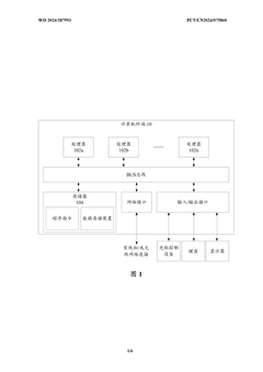
Quantum error correction device and method
PatentPendingKR1020240069597A
Innovation
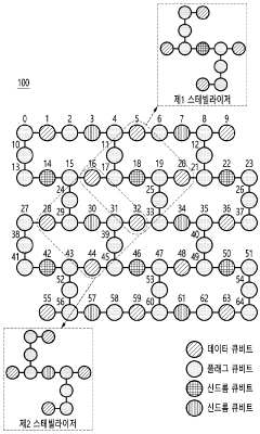
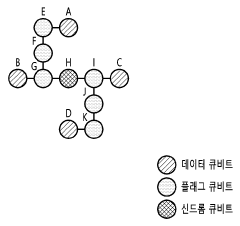
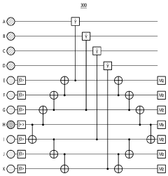
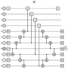
- A quantum error correction apparatus and method that utilizes a heavy-hex grid structure, involving data qubits, flag qubits, and syndrome qubits, with interactions through controlled NOT, controlled-Y, and Hadamard operators to detect and correct errors in a heavy-hex lattice.
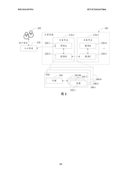
Quantum error correction processing method and apparatus, and computer device
PatentWO2024187993A1
Innovation
- By constructing a noise model of the quantum chip to represent the probability of independent errors and correlated errors during the operation of the quantum chip, quantum error correction simulations are performed to improve the accuracy and effect of error correction.
Quantum Supply Chain Analysis
The quantum computing supply chain represents a complex ecosystem of material suppliers, equipment manufacturers, and specialized service providers that collectively enable the development and operation of quantum computing systems. For quantum error correction (QEC) implementation, this supply chain faces unique challenges due to the stringent requirements for qubit coherence.
Primary materials suppliers in the quantum supply chain include ultra-high purity silicon manufacturers, specialized metal deposition companies, and cryogenic equipment providers. These suppliers must maintain exceptional quality standards as even minor impurities can significantly impact qubit coherence times. The supply chain currently exhibits significant concentration risk, with only a handful of companies capable of producing materials that meet quantum-grade specifications.
Fabrication equipment represents another critical segment of the quantum supply chain. Advanced lithography systems, atomic layer deposition tools, and specialized testing equipment form the backbone of qubit manufacturing infrastructure. Companies like Oxford Instruments, Bluefors, and Keysight Technologies have established themselves as key players in this segment, though capacity constraints remain a persistent challenge.
Geographic distribution of the quantum supply chain reveals concerning vulnerabilities. Critical materials and components are often sourced from regions with geopolitical tensions, creating potential disruption risks. North America and Europe lead in system integration capabilities, while Asia dominates in certain specialized materials production, creating interdependencies that could impact resilience.
Supply chain bottlenecks for coherence-enhancing materials include limited availability of isotopically purified silicon, specialized superconducting metals like niobium and aluminum with ultra-low impurity levels, and high-performance cryogenic systems. These constraints have created extended lead times, sometimes exceeding 12-18 months for critical components.
Vertical integration strategies are emerging among leading quantum computing companies seeking to secure their supply chains. IBM, Google, and Rigetti have invested in developing in-house capabilities for certain critical processes, though complete vertical integration remains economically unfeasible due to the specialized nature of many components.
The quantum supply chain requires significant maturation to support large-scale QEC implementation. Standardization efforts, diversification of supplier networks, and investment in manufacturing capacity represent critical priorities for improving supply chain resilience and enabling the transition from research-scale to production-scale quantum systems.
Scalability Considerations for QEC Implementation
Implementing quantum error correction (QEC) at scale presents significant challenges that must be addressed for practical quantum computing systems. The physical footprint of error-corrected qubits grows substantially compared to non-error-corrected systems, as each logical qubit may require tens or hundreds of physical qubits. This spatial requirement necessitates careful consideration of chip architecture and layout to maintain qubit coherence while accommodating the increased density.
Material selection becomes increasingly critical at scale, as variations in substrate properties can lead to inconsistent qubit performance across large arrays. Uniform material quality must be maintained throughout fabrication processes that extend to larger wafer sizes. Recent advances in epitaxial growth techniques have shown promise in achieving the necessary homogeneity for scaled systems, with defect densities reduced by orders of magnitude compared to earlier approaches.
Fabrication precision must scale proportionally with system size, as systematic errors can compound across larger qubit arrays. Advanced lithography techniques with sub-10nm precision are being developed specifically for quantum computing applications, enabling more consistent qubit parameters across chips. These techniques must be compatible with materials that preserve long coherence times, creating a complex optimization challenge.
Wiring and control line routing present particular challenges for scaled QEC implementations. As qubit counts increase, the density of control and readout lines can introduce crosstalk and heating effects that degrade coherence. Three-dimensional integration approaches, including through-silicon vias and flip-chip bonding, are being explored to address these interconnect challenges while maintaining thermal performance.
Thermal management becomes exponentially more complex in scaled systems, as heat generated by control electronics and measurement apparatus can significantly impact qubit coherence. Novel cooling strategies, including localized refrigeration and superconducting thermal isolation structures, are being developed to maintain uniform, ultra-low temperatures across larger qubit arrays.
Standardization of fabrication processes represents another crucial aspect of scalability. Current laboratory-scale fabrication often relies on customized processes that vary between research groups. Transitioning to industrial-scale production requires establishing reproducible fabrication protocols that maintain coherence properties while enabling higher throughput and yield. Several quantum hardware companies have begun developing proprietary process design kits specifically optimized for maintaining coherence in scaled QEC implementations.
Unlock deeper insights with Patsnap Eureka Quick Research — get a full tech report to explore trends and direct your research. Try now!
Generate Your Research Report Instantly with AI Agent
Supercharge your innovation with Patsnap Eureka AI Agent Platform!