Scalable Wiring And Packaging For Multi-Qubit QEC Arrays
SEP 2, 20259 MIN READ
Generate Your Research Report Instantly with AI Agent
Patsnap Eureka helps you evaluate technical feasibility & market potential.
Quantum Error Correction Wiring Background and Objectives
Quantum Error Correction (QEC) has emerged as a critical technology for realizing fault-tolerant quantum computing systems capable of executing complex quantum algorithms. The evolution of QEC techniques has progressed significantly since the theoretical foundations were established in the mid-1990s, with Peter Shor's and Andrew Steane's pioneering work on quantum error-correcting codes. These early developments laid the groundwork for protecting quantum information against decoherence and operational errors that inevitably affect quantum systems.
The fundamental challenge in quantum computing stems from the fragility of quantum states, which are highly susceptible to environmental noise and control imprecisions. As quantum systems scale beyond a few qubits, the probability of errors occurring during computation increases exponentially, making error correction an absolute necessity for practical quantum computing applications.
The technical objective of scalable wiring and packaging for multi-qubit QEC arrays addresses one of the most significant bottlenecks in implementing practical quantum error correction. Current QEC protocols typically require multiple physical qubits to encode a single logical qubit, with surface codes demanding upwards of 50-1000 physical qubits per logical qubit depending on the desired error suppression level.
This scaling requirement creates an immense engineering challenge: how to efficiently connect, control, and read out thousands or millions of qubits while maintaining quantum coherence. Traditional wiring approaches face fundamental limitations as qubit counts increase, including thermal management issues, crosstalk between control lines, and physical space constraints within cryogenic environments.
Recent technological trends point toward integrated approaches that combine classical control electronics with quantum processing elements, employing advanced materials and novel fabrication techniques. Superconducting interconnects, through-silicon vias, and flip-chip bonding have shown promise in experimental demonstrations, though significant challenges remain in scaling these solutions to the level required for fault-tolerant quantum computation.
The goal of current research in this domain is to develop wiring and packaging architectures that can scale to support millions of physical qubits while maintaining high-fidelity quantum operations. This includes minimizing the footprint of control wiring, reducing thermal loads on cryogenic systems, and ensuring signal integrity across all control channels.
Success in this area would represent a critical milestone toward practical quantum computing, enabling the implementation of complex quantum algorithms with real-world applications in fields such as cryptography, materials science, and pharmaceutical development. The convergence of quantum physics, materials science, electrical engineering, and cryogenic technologies will be essential to overcome these challenges and realize the full potential of quantum error correction.
Market Analysis for Scalable Quantum Computing Systems
The quantum computing market is experiencing unprecedented growth, with projections indicating a compound annual growth rate of 25-30% over the next decade. This surge is primarily driven by increasing investments from both private and governmental sectors, recognizing the transformative potential of quantum technologies across industries. The global quantum computing market, valued at approximately $500 million in 2022, is expected to reach $1.7 billion by 2026 and potentially exceed $10 billion by 2030, according to recent industry analyses.
Scalable wiring and packaging solutions for multi-qubit quantum error correction (QEC) arrays represent a critical segment within this expanding market. As quantum systems transition from experimental setups with dozens of qubits to practical systems requiring thousands or millions of qubits, the demand for sophisticated wiring and packaging technologies is intensifying. This segment is projected to grow at an even faster rate than the overall quantum computing market, potentially reaching 35-40% CAGR in the next five years.
The primary market drivers for scalable wiring and packaging solutions include the increasing focus on quantum advantage demonstrations, the growing need for error-corrected quantum systems, and the push toward quantum supremacy in solving complex computational problems. Financial services, pharmaceuticals, materials science, and cybersecurity sectors are showing particular interest in quantum computing applications, creating substantial demand for scalable quantum hardware.
Current market challenges include the high cost of specialized materials required for quantum-compatible wiring, technical difficulties in maintaining quantum coherence at scale, and the limited supplier ecosystem for quantum-specific packaging solutions. These factors create significant entry barriers but also present opportunities for companies that can develop cost-effective, reliable solutions.
Regional analysis reveals North America leading the market with approximately 45% share, followed by Europe at 30% and Asia-Pacific at 20%. However, China's accelerated investments in quantum technologies are expected to shift this distribution in the coming years. Government initiatives like the U.S. National Quantum Initiative, the EU Quantum Flagship program, and China's national strategy for quantum information sciences are providing substantial funding and creating favorable market conditions.
The customer landscape is currently dominated by research institutions and national laboratories, but enterprise adoption is accelerating, particularly among Fortune 500 companies establishing quantum computing divisions. This shift from research-focused to commercial applications is expected to dramatically expand the addressable market for scalable quantum hardware solutions over the next three to five years.
Current Challenges in Multi-Qubit Array Interconnects
The interconnection challenge in multi-qubit quantum error correction (QEC) arrays represents one of the most significant bottlenecks in scaling quantum computing systems. As quantum processors scale beyond tens of qubits toward the thousands or millions needed for fault-tolerant quantum computing, the wiring complexity increases exponentially, creating severe engineering constraints.
Current wiring approaches typically rely on microwave coaxial cables or flexible circuits that connect to individual qubits. These methods become physically untenable at larger scales due to thermal management issues, signal integrity degradation, and spatial constraints. For instance, a 1,000-qubit processor using conventional wiring would require thousands of control lines, creating an impractical "wiring jungle" that introduces crosstalk and heat loads.
Thermal management presents a particular challenge as quantum systems operate at millikelvin temperatures. Each physical wire introduces heat load into the dilution refrigerator, with current technology limiting the number of wires that can be accommodated while maintaining the required cryogenic environment. This creates a fundamental scaling barrier that conventional approaches cannot overcome.
Signal integrity degradation represents another critical challenge. As wiring density increases, crosstalk between adjacent control lines becomes more pronounced, leading to higher error rates and reduced qubit coherence times. Current shielding techniques become ineffective at the densities required for large-scale QEC implementations.
Packaging constraints further complicate the interconnect problem. The physical space available within dilution refrigerators is severely limited, yet must accommodate increasingly complex wiring harnesses. Traditional packaging approaches from semiconductor industries cannot be directly applied due to the unique thermal and electromagnetic requirements of quantum systems.
Manufacturing scalability presents additional hurdles. Current wiring solutions often involve labor-intensive manual assembly processes that are error-prone and difficult to scale. The transition to automated manufacturing processes is hampered by the precision requirements and specialized materials needed for quantum interconnects.
Material compatibility issues further restrict available solutions. Materials must maintain their electrical and mechanical properties at cryogenic temperatures while generating minimal thermal noise. Many conventional electronic materials exhibit undesirable properties at quantum operating temperatures, limiting the design space for interconnect solutions.
Existing Multi-Qubit Wiring Architectures
01 Scalable interconnect architectures for quantum processors
Advanced interconnect architectures are essential for scaling multi-qubit arrays. These designs focus on minimizing crosstalk between qubits while maintaining signal integrity across the quantum processor. Specialized wiring configurations allow for efficient control and readout of large qubit arrays, incorporating multi-layer routing techniques that can accommodate the increasing complexity of quantum circuits while maintaining quantum coherence.- Scalable interconnect architectures for quantum processors: Advanced interconnect architectures are essential for scaling multi-qubit arrays. These designs focus on minimizing crosstalk between qubits while maintaining signal integrity across the quantum processor. Specialized routing techniques and materials are employed to create dense yet functional wiring systems that can support increasing numbers of qubits without degrading quantum coherence or gate fidelity. These architectures often incorporate hierarchical designs that separate control signals from measurement paths to optimize performance.
- Cryogenic packaging solutions for quantum computing: Quantum computing systems require specialized packaging that can operate at extremely low temperatures. These cryogenic packaging solutions address thermal management challenges while providing sufficient electrical connections to control and read out multiple qubits. Materials with matched thermal expansion coefficients and specialized bonding techniques are used to maintain structural integrity during thermal cycling. The packaging designs also incorporate electromagnetic shielding to protect sensitive quantum states from external interference while facilitating scalability to larger qubit arrays.
- 3D integration techniques for quantum processor scaling: Three-dimensional integration approaches enable higher qubit densities by stacking multiple layers of quantum processing elements. These techniques utilize through-silicon vias (TSVs), flip-chip bonding, and interposer technologies to create compact yet functional multi-qubit arrays. The 3D architecture separates the quantum processing layer from control electronics, allowing for better isolation of qubits from noise sources while maximizing connectivity. This approach addresses key scalability challenges by optimizing the use of available space and reducing signal path lengths.
- Multiplexed control and readout systems: Multiplexing technologies are crucial for scaling quantum systems by reducing the number of physical connections required to control large qubit arrays. These systems employ frequency-division, time-division, or code-division multiplexing to address multiple qubits through shared signal paths. Advanced signal processing techniques are implemented to maintain high-fidelity control while minimizing crosstalk between channels. The multiplexed architecture significantly reduces wiring complexity and heat load in cryogenic environments, enabling practical scaling to larger qubit counts.
- Modular quantum processor architectures: Modular approaches to quantum processor design enable scalability by connecting smaller, well-characterized qubit modules into larger systems. These architectures incorporate standardized interfaces between modules and utilize quantum communication channels to establish entanglement between physically separated qubit arrays. The modular design facilitates manufacturing, testing, and system upgrades while providing a path to fault-tolerant quantum computing. Specialized interconnects between modules maintain quantum coherence while supporting the classical control infrastructure needed for large-scale operation.
02 3D packaging solutions for quantum computing systems
Three-dimensional packaging technologies enable higher qubit densities and improved thermal management in quantum computing systems. These solutions integrate multiple qubit layers with control electronics through vertical interconnects, allowing for more efficient use of space while addressing the challenges of heat dissipation. Advanced materials and fabrication techniques are employed to maintain quantum coherence while scaling to larger qubit counts.Expand Specific Solutions03 Cryogenic wiring and signal delivery systems
Specialized wiring systems designed for cryogenic environments are crucial for quantum computing operations. These systems must maintain signal fidelity while minimizing heat load on the quantum processor. Advanced materials and filtering techniques are employed to reduce thermal noise and electromagnetic interference. The designs incorporate careful impedance matching and thermal anchoring to ensure reliable operation at millikelvin temperatures required for superconducting qubits.Expand Specific Solutions04 Modular qubit array architectures
Modular approaches to quantum processor design enable scalable systems through interconnected qubit modules. These architectures incorporate standardized interfaces between modules, allowing for incremental scaling of quantum processors. The modular design facilitates easier testing, maintenance, and upgrades while providing a pathway to fault-tolerant quantum computing. Specialized interconnects between modules maintain quantum coherence while enabling distributed quantum processing across multiple qubit arrays.Expand Specific Solutions05 Integrated control electronics for large-scale qubit arrays
Integration of control electronics with qubit arrays is essential for scaling quantum processors. These systems incorporate multiplexing techniques to reduce the number of control lines required per qubit, addressing the wiring bottleneck in large-scale quantum systems. Advanced CMOS integration with quantum circuits enables more efficient control and readout of multiple qubits. The designs balance proximity of control electronics with the need to isolate sensitive quantum states from electronic noise and interference.Expand Specific Solutions
Leading Organizations in Quantum Packaging Solutions
The quantum error correction (QEC) wiring and packaging landscape is in an early development stage, with market growth accelerating as quantum computing transitions from research to practical applications. Major technology players like IBM, Google, and D-Wave are competing alongside specialized quantum startups such as IQM and Quantum Motion Technologies. Academic institutions including MIT, Delft University, and University of Science & Technology of China contribute significant research advancements. The technical challenge of scaling interconnects for multi-qubit arrays represents a critical bottleneck in quantum computing development. Companies like Origin Quantum, Fujitsu, and Toshiba are developing proprietary packaging solutions, while semiconductor specialists including KIOXIA, Infineon, and Siliconware Precision bring manufacturing expertise to address the unique requirements of quantum hardware integration.
Google LLC
Technical Solution: Google has developed a comprehensive approach to scalable wiring and packaging for quantum error correction (QEC) arrays through their Sycamore and subsequent quantum processors. Their architecture employs a 2D grid arrangement of qubits with nearest-neighbor connectivity, optimized for surface code implementation. For wiring challenges, Google utilizes a multi-layer interposer design that routes control and readout signals from room temperature electronics to the quantum chip at millikelvin temperatures. This interposer incorporates superconducting traces and carefully designed signal paths to minimize crosstalk and maintain signal integrity[3]. Google's packaging solution features a flip-chip bonding technique where the quantum processor is connected to an interposer using indium bump bonds, allowing for high-density connections while maintaining the necessary thermal and mechanical properties for cryogenic operation. Their design includes integrated attenuators and filters directly in the package to reduce noise and improve qubit coherence. Google has also pioneered automated calibration systems that can handle the increasing complexity of larger qubit arrays, addressing the challenge of tuning multiple qubits simultaneously[4].
Strengths: Google's interposer design efficiently handles the complex routing requirements for large qubit arrays. Their integrated filtering approach improves signal quality and qubit performance. The automated calibration systems enable practical scaling to larger qubit counts. Weaknesses: The current architecture may face limitations in scaling beyond several hundred qubits due to the increasing complexity of the 2D routing approach, and the flip-chip bonding process introduces potential yield challenges at larger scales.
Delft University of Technology
Technical Solution: Delft University of Technology has pioneered a unique approach to scalable wiring and packaging for multi-qubit QEC arrays through their "quantum socket" architecture. Their solution addresses the fundamental challenge of connecting room-temperature control electronics to quantum chips operating at millikelvin temperatures. Delft's design utilizes a modular approach with a specialized three-dimensional wiring scheme that minimizes thermal load while maximizing signal integrity. Their quantum socket incorporates spring-loaded micro-pins that make reliable contact with the quantum chip, allowing for easy replacement and testing of different quantum processors without disturbing the entire cryogenic setup[5]. For larger qubit arrays, Delft has developed a segmented architecture where multiple smaller quantum chips are interconnected using superconducting pathways, effectively creating a distributed quantum computing system. This approach significantly reduces the wiring complexity that would otherwise increase quadratically with qubit count. Their packaging solution also incorporates specialized electromagnetic shielding techniques to protect sensitive qubits from environmental noise, including a multi-layer shielding approach that addresses both static and dynamic magnetic fields[6].
Strengths: The modular socket approach allows for flexible testing and iterative improvement of quantum processors. The segmented architecture provides a practical path to scaling beyond the limitations of single-chip designs. Their specialized shielding techniques effectively address environmental noise issues. Weaknesses: The mechanical complexity of the spring-loaded contacts may introduce reliability challenges at scale, and the distributed architecture introduces additional synchronization and calibration requirements that must be carefully managed.
Critical Patents in Scalable Quantum Interconnect Design
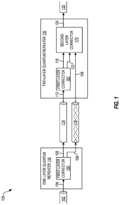
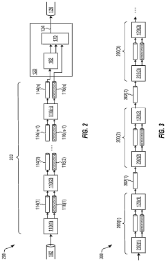
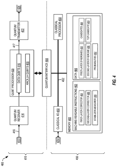
Quantum repeaters for concatenated quantum error correction, and associated methods
PatentActiveUS20230206110A1
Innovation
- The implementation of quantum repeaters using concatenated error correction codes, where a second-layer logical qubit is block-encoded by a plurality of physical qubits according to a second-layer code concatenated with a first-layer code, allowing for the detection and correction of errors through first-layer and second-layer stabilizer measurements, reducing the need for resources and noise introduction.
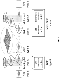
Quantum repeaters for concatenated quantum error correction, and associated methods
PatentWO2022039818A2
Innovation
- The implementation of a hybrid quantum repeater architecture using concatenated quantum error correction with continuous-variable bosonic encoding at the lower level and discrete-variable encoding at the higher level, specifically employing the Gottesman-Kitaev-Preskill (GKP) code and Steane codes, to correct errors and extend transmission distances with reduced resource usage.

Cryogenic Engineering Considerations
Cryogenic engineering represents a critical challenge in the development of scalable wiring and packaging solutions for multi-qubit quantum error correction (QEC) arrays. The operational requirements of quantum computers necessitate extremely low temperatures, typically in the millikelvin range, to maintain quantum coherence and minimize thermal noise that could disrupt qubit operations.
The thermal management of signal lines presents a significant engineering hurdle. Each additional control wire introduces heat load into the system, creating a delicate balance between providing sufficient control channels and maintaining the required cryogenic temperatures. Current approaches employ careful material selection, including superconducting materials like niobium and aluminum, which offer zero electrical resistance at low temperatures while minimizing thermal conductivity.
Thermal anchoring techniques have evolved substantially, with staged cooling strategies becoming standard practice. These involve thermally anchoring wires at multiple temperature stages (e.g., 4K, 1K, 100mK, and 20mK), effectively creating thermal gradients that minimize heat flow to the coldest stage where qubits reside. Advanced filtering schemes are implemented at each stage to reduce electromagnetic interference while managing heat loads.
Cryogenic packaging materials must address competing requirements of thermal isolation, electrical performance, and mechanical stability. Specialized materials such as low-loss dielectrics, thermally matched composites, and custom-designed alloys are increasingly being developed specifically for quantum computing applications. These materials must maintain consistent properties across extreme temperature ranges while providing suitable platforms for complex integrated circuits.
Vacuum and radiation shielding considerations further complicate the engineering landscape. The cryogenic environment must be protected from both external thermal radiation and electromagnetic interference, requiring sophisticated multi-layer shielding designs. Recent innovations include integrated radiation shields that double as thermal anchors, optimizing both space and performance in increasingly dense qubit arrays.
Refrigeration capacity scaling represents perhaps the most fundamental limitation to quantum system growth. Current dilution refrigerators typically provide cooling power measured in microwatts at base temperature, severely constraining the number of control lines and active components that can be accommodated. Industry leaders are pursuing parallel development of higher-capacity cooling systems alongside more thermally efficient wiring solutions to address this bottleneck.
Emerging approaches include on-chip multiplexing to reduce external wiring requirements, superconducting through-silicon vias (TSVs) for vertical integration, and novel cooling architectures that distribute refrigeration capacity more effectively throughout the system. These innovations aim to support the transition from current experimental systems to practical, error-corrected quantum computers requiring thousands or millions of physical qubits.
Materials Science Innovations for Quantum Interconnects
Materials science innovations are driving significant advancements in quantum interconnect technologies, addressing the critical challenges in scaling quantum computing systems. Traditional metallic interconnects face fundamental limitations when applied to quantum circuits, particularly in maintaining quantum coherence while efficiently transmitting signals at cryogenic temperatures. Recent breakthroughs in superconducting materials have enabled the development of interconnects with near-zero resistance and minimal thermal noise, crucial for preserving the delicate quantum states in multi-qubit arrays.
Novel composite materials combining superconducting elements with specialized insulators have demonstrated superior performance in quantum error correction (QEC) architectures. These materials maintain their superconducting properties at operating temperatures below 100 mK while providing the necessary electromagnetic isolation between adjacent qubits. Researchers have achieved significant progress in developing thin-film superconducting materials that can be deposited with nanometer precision, enabling complex routing schemes for dense qubit arrays.
Advances in materials processing techniques have facilitated the integration of heterogeneous material systems within quantum packages. Particularly noteworthy is the development of low-loss dielectric materials that minimize signal attenuation and crosstalk between quantum interconnects. These materials exhibit exceptionally low tangent loss factors (tan δ < 10^-5) at microwave frequencies and cryogenic temperatures, preserving signal integrity across the quantum processor.
The interface between classical and quantum domains represents another frontier where materials innovation is essential. Novel metamaterials engineered at the nanoscale have demonstrated the ability to efficiently convert between different signal modalities while maintaining quantum coherence. These materials incorporate precisely engineered structures that can manipulate electromagnetic fields at the quantum level, enabling more efficient control and readout of qubit states.
Thermal management presents a significant challenge in quantum interconnect design, as heat dissipation can destroy quantum coherence. Recent developments in phononic crystals and engineered thermal barrier materials have shown promise in directing heat flow away from sensitive quantum elements. These materials exploit quantum confinement effects to create highly directional thermal conductivity, protecting qubits from thermal noise while allowing efficient heat extraction through designated pathways.
Looking forward, two-dimensional materials such as graphene and hexagonal boron nitride are emerging as promising candidates for next-generation quantum interconnects. Their unique electronic properties, atomically precise interfaces, and compatibility with existing fabrication techniques make them particularly attractive for scaling quantum systems beyond current limitations. Initial demonstrations have shown these materials can maintain quantum coherence over longer distances than conventional interconnects, potentially enabling more complex QEC implementations.
Unlock deeper insights with Patsnap Eureka Quick Research — get a full tech report to explore trends and direct your research. Try now!
Generate Your Research Report Instantly with AI Agent
Supercharge your innovation with Patsnap Eureka AI Agent Platform!