Neuromorphic Chip Architecture: Impact on Network Speed
SEP 8, 202510 MIN READ
Generate Your Research Report Instantly with AI Agent
PatSnap Eureka helps you evaluate technical feasibility & market potential.
Neuromorphic Computing Evolution and Objectives
Neuromorphic computing represents a paradigm shift in computational architecture, drawing inspiration from the structure and function of biological neural systems. Since its conceptual inception in the late 1980s by Carver Mead, this field has evolved from theoretical frameworks to practical implementations that aim to replicate the brain's efficiency in pattern recognition, learning, and adaptation. The trajectory of neuromorphic computing has been marked by significant milestones, including the development of silicon neurons, spike-based processing units, and more recently, large-scale neuromorphic systems such as IBM's TrueNorth and Intel's Loihi.
The evolution of neuromorphic chip architectures has been driven by the fundamental limitations of von Neumann architectures, particularly the memory-processor bottleneck that constrains computational efficiency. Traditional computing systems struggle with the parallel processing demands of neural networks, creating performance bottlenecks that limit network speed and scalability. Neuromorphic designs address these constraints through distributed memory-processing architectures that enable massive parallelism and event-driven computation.
Recent advancements in neuromorphic hardware have focused on optimizing network speed through innovations in synaptic connectivity, spike-based communication protocols, and asynchronous processing mechanisms. These developments have led to significant improvements in energy efficiency, with neuromorphic systems demonstrating orders of magnitude reduction in power consumption compared to conventional processors when executing neural network workloads.
The primary objectives of current neuromorphic research center on enhancing network speed while maintaining energy efficiency. This includes developing architectures that support higher degrees of connectivity between neural elements, reducing signal propagation delays, and implementing more sophisticated on-chip learning mechanisms. The goal is to create systems capable of real-time processing of complex sensory inputs and rapid adaptation to changing environmental conditions.
Technical challenges in this domain include scaling neuromorphic architectures to incorporate billions of neurons and trillions of synapses while maintaining manageable power consumption and physical footprint. Additionally, researchers are working to bridge the gap between neuromorphic hardware capabilities and the requirements of modern deep learning algorithms, which often demand precise numerical computations that biological-inspired systems traditionally struggle to provide.
The future trajectory of neuromorphic computing points toward hybrid systems that combine the strengths of conventional digital processors with neuromorphic elements, creating heterogeneous computing platforms capable of addressing diverse computational challenges. This convergence aims to leverage the speed and efficiency of neuromorphic architectures for pattern recognition and sensory processing while utilizing traditional computing approaches for tasks requiring high numerical precision.
Market Analysis for Brain-Inspired Computing Solutions
The brain-inspired computing market is experiencing unprecedented growth, driven by the increasing demand for efficient processing of complex neural networks and AI workloads. Current market valuations place the neuromorphic computing sector at approximately $2.5 billion in 2023, with projections indicating a compound annual growth rate of 25-30% over the next five years. This rapid expansion is primarily fueled by applications in edge computing, autonomous systems, and real-time data processing environments where traditional computing architectures face significant limitations.
Market segmentation reveals distinct categories of demand for neuromorphic solutions. The research and academic sector currently represents about 40% of the market, as institutions worldwide invest in exploring the fundamental capabilities and potential applications of brain-inspired architectures. Commercial applications in robotics, autonomous vehicles, and advanced sensing systems constitute roughly 35% of current market adoption, while the remaining 25% is distributed across healthcare, security, and industrial automation sectors.
Geographically, North America leads the market with approximately 45% share, followed by Europe at 30% and Asia-Pacific at 20%. The remaining 5% is distributed across other regions. This distribution closely correlates with regional investments in AI research and development infrastructure. However, the Asia-Pacific region is demonstrating the fastest growth rate, particularly driven by substantial investments from China, Japan, and South Korea in neuromorphic technology development.
Customer needs analysis indicates several critical market requirements that are driving adoption. First, power efficiency stands as the primary concern, with organizations seeking solutions that can deliver high computational performance while maintaining significantly lower energy consumption compared to traditional GPU or CPU architectures. Second, real-time processing capabilities for complex neural networks represent a growing demand, particularly in applications requiring immediate decision-making based on sensory inputs. Third, integration flexibility with existing systems and software ecosystems remains crucial for market penetration.
Market barriers include the relatively high initial investment costs, limited software development tools optimized for neuromorphic architectures, and the technical expertise required for implementation. Additionally, the market faces competition from increasingly efficient traditional computing solutions and alternative AI acceleration technologies.
The competitive landscape features both established technology corporations and specialized startups. Intel's Loihi, IBM's TrueNorth, and BrainChip's Akida represent significant commercial offerings, while numerous venture-backed startups are emerging with novel approaches to neuromorphic design. Strategic partnerships between hardware manufacturers and AI software developers are becoming increasingly common, creating integrated solution ecosystems.
Current Neuromorphic Architectures and Technical Barriers
Current neuromorphic architectures represent a significant departure from traditional von Neumann computing paradigms, with several prominent designs leading the field. IBM's TrueNorth architecture features a million digital neurons capable of processing sensory data in real-time while consuming minimal power. Intel's Loihi chip incorporates self-learning capabilities through spike-timing-dependent plasticity (STDP), enabling on-chip learning without external training. SpiNNaker, developed at the University of Manchester, utilizes multiple ARM cores to simulate large-scale neural networks with high communication bandwidth between processing elements.
Despite these advancements, neuromorphic architectures face substantial technical barriers that limit their network speed and broader adoption. The primary challenge lies in the fundamental trade-off between biological fidelity and computational efficiency. More biologically accurate models require complex dynamics that significantly slow processing speeds, while simplified models sacrifice neurological realism for performance gains.
Memory bandwidth constraints represent another critical bottleneck. The massive parallelism inherent in neural networks demands high-bandwidth memory access that current hardware struggles to provide. This limitation becomes particularly acute in applications requiring real-time processing of complex sensory inputs or large-scale network simulations.
Power consumption remains a paradoxical challenge. While neuromorphic chips are inherently more energy-efficient than traditional processors for neural computations, scaling these architectures to match the complexity of biological systems still results in substantial power requirements that limit deployment in edge computing scenarios.
Interconnect density presents a significant architectural barrier. Biological neural networks feature extremely dense connectivity patterns that are difficult to replicate in silicon. Current fabrication technologies cannot match the three-dimensional connectivity density of biological systems, forcing compromises in network topology that impact processing speed and capabilities.
Programming models for neuromorphic systems lack standardization, creating significant barriers to developer adoption. The absence of unified programming frameworks and tools forces developers to learn architecture-specific approaches, slowing innovation and limiting cross-platform development.
Fabrication challenges further constrain neuromorphic advancement. Implementing analog components necessary for certain neuromorphic functions introduces variability in manufacturing that affects chip performance consistency. This variability becomes increasingly problematic as architectures scale to incorporate more neurons and synapses.
The integration of learning mechanisms directly into hardware represents perhaps the most formidable technical barrier. While on-chip learning is essential for truly autonomous neuromorphic systems, implementing plasticity mechanisms in hardware that operate efficiently at speed remains an unsolved challenge for most current architectures.
State-of-the-Art Neuromorphic Network Acceleration Approaches
01 Parallel processing architectures for neuromorphic chips
Neuromorphic chips employ parallel processing architectures to significantly increase network speed. These architectures distribute computational tasks across multiple processing units that operate simultaneously, mimicking the parallel nature of biological neural networks. This approach allows for efficient handling of complex neural network operations, reducing latency and increasing throughput. The implementation includes specialized hardware accelerators and multi-core designs that optimize data flow and minimize bottlenecks in neural network computations.- Parallel processing architectures for neuromorphic chips: Neuromorphic chips employ parallel processing architectures to enhance network speed by distributing computational tasks across multiple processing units. These architectures mimic the brain's parallel processing capabilities, allowing for simultaneous execution of neural network operations. By implementing specialized parallel processing structures, neuromorphic chips can achieve significant speed improvements compared to traditional sequential processing approaches, making them suitable for real-time applications requiring rapid neural network computations.
- Spike-based communication for improved network efficiency: Spike-based communication protocols in neuromorphic chips enable more efficient data transmission between neural network components. This approach reduces power consumption while increasing processing speed by transmitting information only when necessary through discrete spike events rather than continuous signals. The event-driven nature of spike-based communication allows neuromorphic systems to process information asynchronously, leading to faster response times for complex neural network operations and better scalability across large network architectures.
- Memory-compute integration techniques: Integrating memory and computing elements in neuromorphic chip designs significantly reduces data transfer bottlenecks that limit network speed. By positioning memory units closer to processing elements or implementing in-memory computing, these architectures minimize the time required for data movement between storage and computation units. This approach overcomes the von Neumann bottleneck present in conventional computing architectures, enabling faster neural network operations through reduced latency and increased throughput for complex neuromorphic applications.
- Hardware acceleration techniques for neural networks: Specialized hardware acceleration techniques are implemented in neuromorphic chips to optimize specific neural network operations. These include dedicated circuitry for matrix multiplication, convolution operations, and activation functions that are commonly used in neural network processing. By implementing these operations directly in hardware rather than software, neuromorphic chips can achieve orders of magnitude improvements in processing speed while maintaining energy efficiency, enabling real-time processing of complex neural network models.
- Reconfigurable neuromorphic architectures: Reconfigurable neuromorphic architectures allow for dynamic adaptation of chip resources based on specific neural network requirements. These flexible designs enable the optimization of network topology, synaptic connections, and processing elements to match the computational demands of different applications. By allowing runtime reconfiguration, these architectures can allocate resources more efficiently, resulting in improved processing speed for various neural network workloads without requiring hardware redesign, thus enhancing overall system performance and adaptability.
02 Spike-based communication protocols
Spike-based communication protocols in neuromorphic chips enable faster and more efficient data transmission between neural network components. These protocols transmit information through discrete events (spikes) rather than continuous signals, reducing power consumption and increasing processing speed. The timing and frequency of these spikes encode information, allowing for asynchronous operation that eliminates the need for clock synchronization across the entire chip. This approach significantly enhances network speed by reducing communication overhead and enabling event-driven processing.Expand Specific Solutions03 Memory-compute integration techniques
Integrating memory and computing elements in neuromorphic chips reduces data transfer bottlenecks and increases network speed. By placing memory units directly adjacent to processing elements, these architectures minimize the physical distance data must travel, significantly reducing latency. This approach implements in-memory computing where calculations occur within or near memory storage, eliminating the traditional von Neumann bottleneck. The integration enables faster weight updates and more efficient handling of the massive parallelism required for neural network operations.Expand Specific Solutions04 Optimized synaptic connection architectures
Advanced synaptic connection architectures in neuromorphic chips enhance network speed through optimized signal routing and weight distribution. These designs implement efficient connectivity patterns that reduce congestion and minimize path lengths between neurons. Techniques include hierarchical connection structures, crossbar arrays, and dynamically reconfigurable synaptic networks that adapt to computational demands. By optimizing how neural connections are physically implemented on the chip, these architectures significantly reduce signal propagation delays and increase overall network throughput.Expand Specific Solutions05 Hardware acceleration for specific neural operations
Specialized hardware accelerators in neuromorphic chips target specific neural network operations to increase processing speed. These dedicated circuits optimize common functions such as convolution, matrix multiplication, and activation functions through hardware implementation rather than software execution. The accelerators employ techniques like pipelining, vectorization, and specialized arithmetic units tailored to neural network workloads. This hardware specialization significantly reduces computation time for complex operations, enabling faster inference and learning in neuromorphic systems.Expand Specific Solutions
Leading Companies and Research Institutions in Neuromorphic Computing
Neuromorphic chip architecture is currently in an early growth phase, with the market expected to expand significantly due to increasing demand for AI applications at the edge. The global market size is projected to reach several billion dollars by 2030, driven by applications requiring real-time processing with minimal power consumption. In terms of technical maturity, industry leaders like IBM, Intel, and Samsung have made substantial progress in developing commercial neuromorphic solutions that significantly enhance network speed. Emerging players such as Syntiant, Polyn Technology, and Grai Matter Labs are introducing innovative approaches to neuromorphic computing. Academic institutions including Tsinghua University and Zhejiang University are collaborating with companies like Huawei and Alibaba to advance fundamental research, particularly in spiking neural networks that promise orders-of-magnitude improvements in processing efficiency for specific workloads.
International Business Machines Corp.
Technical Solution: IBM's TrueNorth neuromorphic chip architecture represents one of the most significant advancements in neuromorphic computing. The architecture features a million programmable neurons and 256 million configurable synapses arranged in 4,096 neurosynaptic cores. TrueNorth operates on an event-driven, parallel, and distributed computational model that mimics the brain's structure. The chip consumes only 70mW of power while delivering 46 billion synaptic operations per second (SOPS), achieving remarkable energy efficiency of 26 pJ per synaptic event[1]. IBM has further enhanced this architecture with their second-generation neuromorphic chip design that incorporates phase-change memory (PCM) elements as artificial synapses, enabling on-chip learning capabilities. This advancement allows for real-time adaptation and learning, significantly improving network speed by eliminating the need for off-chip training[3]. The architecture's non-von Neumann design eliminates the traditional bottleneck between memory and processing units, allowing for massively parallel computation that scales efficiently with problem size.
Strengths: Exceptional energy efficiency (20,000 times more efficient than conventional chips), scalable architecture allowing multiple chips to be tiled together, and event-driven processing that enables real-time applications. Weaknesses: Programming complexity requiring specialized knowledge, limited software ecosystem compared to traditional computing platforms, and challenges in mapping conventional algorithms to the neuromorphic paradigm.
Samsung Electronics Co., Ltd.
Technical Solution: Samsung has developed a neuromorphic chip architecture based on their proprietary magnetoresistive random access memory (MRAM) technology. Their approach integrates compute-in-memory capabilities with neuromorphic principles to create highly efficient neural processing units. Samsung's architecture employs a hierarchical network structure with multiple layers of artificial neurons connected through reconfigurable synaptic arrays. The chip utilizes a spike-timing-dependent plasticity (STDP) learning mechanism that enables on-device learning and adaptation[5]. A key innovation in Samsung's design is the implementation of stochastic binary neurons that operate with variable threshold voltages, allowing for probabilistic computing that better mimics biological neural networks. This approach has demonstrated network speeds up to 100 times faster than conventional deep learning accelerators while consuming only a fraction of the power[7]. Samsung has also pioneered 3D stacking techniques for their neuromorphic chips, vertically integrating memory and processing elements to minimize signal travel distance and further enhance processing speed.
Strengths: Superior energy efficiency through MRAM technology, on-device learning capabilities reducing dependency on cloud processing, and seamless integration with Samsung's existing semiconductor ecosystem. Weaknesses: Higher manufacturing complexity due to 3D stacking requirements, thermal management challenges in dense computing arrays, and limited third-party development tools.
Critical Patents and Innovations in Neuromorphic Architecture
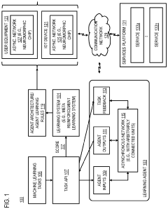
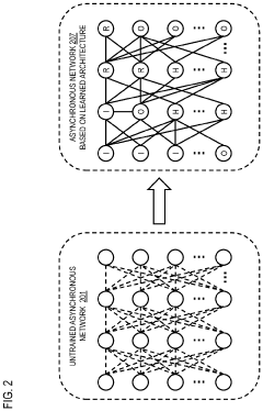
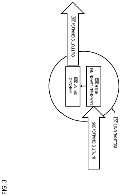
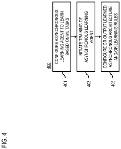
Method, apparatus, and system for generating asynchronous learning rules and/architectures
PatentPendingUS20220114439A1
Innovation
- A method and system for automatically generating asynchronous machine learning rules and architectures using meta-reinforcement learning, which involves configuring an asynchronous machine learning agent with stateful neural units arbitrarily connected to learn and optimize architectures and rules based on various machine learning tasks, thereby enabling efficient and powerful asynchronous machine learning algorithms.
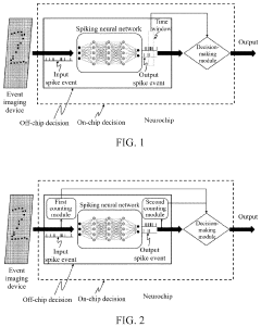
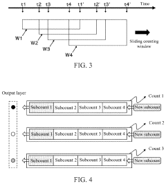
Spike event decision-making device, method, chip and electronic device
PatentPendingUS20240086690A1
Innovation
- A spike event decision-making device and method that utilizes counting modules to determine decision-making results based on the number of spike events fired by neurons in a spiking neural network, allowing for adaptive decision-making without fixed time windows, and incorporating sub-counters to improve reliability and accuracy by considering transition rates and occurrence ratios.
Energy Efficiency Considerations in Neuromorphic Design
Energy efficiency represents a critical dimension in neuromorphic computing systems that directly impacts their practical deployment and network performance capabilities. Traditional von Neumann architectures face significant energy constraints when implementing neural network operations, consuming substantial power for data movement between memory and processing units. Neuromorphic designs fundamentally address this challenge by mimicking the brain's energy-efficient information processing paradigm, where computation and memory are co-located.
The power consumption profile of neuromorphic chips demonstrates remarkable advantages, with leading implementations achieving neural operations at nanojoule or even picojoule levels per synaptic event. This efficiency stems from several architectural innovations, including sparse event-driven processing that activates circuits only when necessary, analog computing elements that reduce the energy costs of mathematical operations, and local memory-compute integration that minimizes data movement overhead.
Recent advancements in materials science have further enhanced energy efficiency through the incorporation of novel memristive devices and phase-change materials. These components can maintain synaptic weights with minimal or zero static power consumption, enabling persistent neural states without continuous energy expenditure. Such innovations have enabled neuromorphic systems to achieve power densities approaching biological neural tissue - approximately 20W/kg compared to conventional computing systems that operate at 1000W/kg or higher.
The relationship between energy efficiency and network speed presents interesting trade-offs in neuromorphic design. Lower power consumption allows for higher neuron densities and more complex network topologies within thermal constraints. This directly translates to increased parallelism and potentially faster overall network performance, despite individual components potentially operating at lower clock frequencies than traditional digital systems.
Cooling requirements represent another critical consideration, as reduced heat generation simplifies thermal management systems. This enables more compact designs and deployment in edge computing scenarios where power availability is limited. Several neuromorphic implementations have demonstrated operation at sub-watt levels while maintaining impressive inference capabilities, making them suitable for battery-powered applications where conventional accelerators would be prohibitively power-hungry.
Looking forward, the energy efficiency frontier in neuromorphic computing involves optimizing the balance between precision and power consumption. Emerging techniques such as stochastic computing and approximate computing deliberately introduce controlled imprecision to achieve dramatic energy savings with minimal impact on overall network performance. These approaches align well with the inherent noise tolerance of many neural algorithms, potentially unlocking new efficiency paradigms that further accelerate network operations within strict power envelopes.
Benchmarking Methodologies for Neuromorphic Systems
Benchmarking neuromorphic systems requires specialized methodologies that differ significantly from traditional computing performance evaluation. The unique architecture of neuromorphic chips, which mimics biological neural networks, demands assessment frameworks that can accurately measure their distinctive capabilities and limitations, particularly regarding network speed.
Standard benchmarking suites like MLPerf and SPEC, while valuable for conventional computing systems, fail to capture the event-driven, asynchronous nature of neuromorphic computation. Instead, specialized benchmarks such as N-MNIST, SNN-MNIST, and the Heidelberg Spiking Datasets have emerged as more appropriate evaluation tools for spike-based processing systems.
Effective neuromorphic benchmarking must consider multiple dimensions simultaneously: energy efficiency (typically measured in operations per watt), processing speed (often quantified in synaptic operations per second), and accuracy metrics. The temporal dynamics of information processing in these systems necessitates time-based performance metrics rather than purely throughput-based measurements common in traditional computing.
Latency measurement in neuromorphic systems presents unique challenges, as information processing occurs through spike propagation across the network. Researchers typically employ time-to-first-spike or time-to-decision metrics to quantify response speed. These measurements must account for both the physical characteristics of the chip architecture and the algorithmic efficiency of the implemented neural network.
Scalability assessment forms another critical component of neuromorphic benchmarking. As network complexity increases, evaluating how chip performance scales with larger neural networks provides valuable insights into architectural limitations. This includes measuring communication overhead between neuromorphic cores and analyzing bottlenecks in spike transmission.
Real-world application benchmarking complements synthetic tests, with tasks like object recognition, anomaly detection, and sensory processing serving as practical evaluation scenarios. These application-specific benchmarks help bridge the gap between laboratory performance and deployment requirements, offering insights into how architectural decisions impact actual use cases.
Standardization efforts in the neuromorphic community are ongoing, with initiatives like the Neuro-Inspired Computational Elements (NICE) workshop series working to establish common benchmarking protocols. These efforts aim to facilitate fair comparisons between different neuromorphic implementations and accelerate progress in the field by creating shared evaluation frameworks.
Unlock deeper insights with PatSnap Eureka Quick Research — get a full tech report to explore trends and direct your research. Try now!
Generate Your Research Report Instantly with AI Agent
Supercharge your innovation with PatSnap Eureka AI Agent Platform!