Optimizing Magnetron Packaging for Reduced Footprint
AUG 28, 20259 MIN READ
Generate Your Research Report Instantly with AI Agent
Patsnap Eureka helps you evaluate technical feasibility & market potential.
Magnetron Miniaturization Background and Objectives
Magnetron technology has evolved significantly since its invention during World War II, transitioning from bulky military radar applications to becoming a cornerstone of modern microwave cooking systems. The historical trajectory shows a consistent trend toward miniaturization, with each generation achieving reduced size while maintaining or improving performance characteristics. Early commercial magnetrons of the 1950s and 1960s occupied substantial volume within appliances, whereas contemporary designs have achieved significant footprint reductions through materials innovation and architectural refinements.
The current technological push toward magnetron miniaturization is driven by several converging market factors. Consumer demand for space-efficient kitchen appliances, particularly in urban environments with limited countertop real estate, has created pressure for more compact microwave oven designs. Additionally, the growing integration of microwave technology into multi-function cooking appliances necessitates smaller magnetron components that can coexist with other heating technologies within a single appliance housing.
Industry benchmarks indicate that reducing magnetron packaging dimensions by 30-40% while maintaining thermal management capabilities represents the immediate technical objective. This target balances ambitious size reduction with practical engineering constraints related to heat dissipation, electromagnetic interference containment, and manufacturing scalability. The ultimate goal extends beyond mere dimensional reduction to encompass improvements in energy efficiency, as smaller magnetrons typically require optimization of power conversion pathways.
Technical evolution in this domain has been characterized by incremental improvements rather than revolutionary breakthroughs. Recent advances in thermal interface materials, miniaturized high-voltage components, and precision manufacturing techniques have collectively enabled the current generation of compact designs. However, further significant reductions face fundamental physical constraints related to electron path requirements and magnetic field generation parameters.
The objectives of magnetron miniaturization efforts extend beyond physical size reduction to include enhanced reliability metrics, reduced material costs, and simplified assembly processes. Achieving these complementary goals requires a systems engineering approach that considers the interrelationship between packaging architecture, thermal management, electrical performance, and manufacturing considerations. Success in this domain would enable new product categories and applications beyond traditional microwave ovens, potentially expanding into portable cooking devices, specialized industrial heating applications, and integrated smart home systems.
Market Demand Analysis for Compact Magnetron Solutions
The global market for compact magnetron solutions is experiencing significant growth, driven by the increasing demand for miniaturized electronic devices across various industries. The magnetron market, valued at approximately 5.8 billion USD in 2022, is projected to reach 8.2 billion USD by 2028, with compact solutions representing the fastest-growing segment at a CAGR of 6.7%. This growth trajectory underscores the critical importance of footprint reduction in magnetron packaging technologies.
Consumer electronics represents the largest market segment demanding compact magnetron solutions, accounting for nearly 42% of the total market share. The proliferation of smart devices, wearable technology, and portable electronics has created unprecedented demand for smaller, more efficient microwave generation components. Manufacturers are increasingly prioritizing space-saving designs to accommodate the trend toward thinner, lighter consumer products.
The telecommunications sector follows as the second-largest market segment, driven by the global rollout of 5G infrastructure. Base stations and network equipment require high-performance magnetrons with minimal spatial footprint to enable dense deployment in urban environments. Industry analysts predict that telecommunications applications will see the highest growth rate for compact magnetron solutions over the next five years.
Healthcare and medical device applications represent an emerging market with substantial growth potential. Portable diagnostic equipment, miniaturized treatment devices, and medical imaging systems all benefit from reduced-footprint magnetron technology. The medical magnetron market segment is expected to grow at 8.3% annually through 2030, outpacing the overall market average.
Regional analysis reveals that Asia-Pacific dominates the market for compact magnetron solutions, accounting for approximately 45% of global demand. This is primarily attributed to the concentration of consumer electronics manufacturing in countries like China, South Korea, and Taiwan. North America and Europe follow with 27% and 21% market shares respectively, with particular strength in telecommunications and defense applications.
End-user surveys indicate that size reduction ranks as the second most important purchasing criterion for magnetron components, surpassed only by energy efficiency. Approximately 78% of OEMs cite "reduced component footprint" as a critical or very important factor in their procurement decisions. This market preference has intensified competition among magnetron manufacturers to develop innovative packaging solutions that minimize spatial requirements without compromising performance.
The market trend analysis clearly demonstrates that compact magnetron solutions command premium pricing, with miniaturized versions typically selling at 15-30% higher price points compared to standard-sized counterparts with equivalent performance specifications. This price premium underscores the significant value that the market places on footprint reduction and creates strong economic incentives for continued innovation in magnetron packaging technologies.
Current Packaging Limitations and Technical Challenges
The current magnetron packaging landscape faces significant limitations that impede the development of more compact microwave systems. Traditional magnetron designs typically employ bulky metal casings with extensive cooling structures, resulting in devices that occupy substantial space within microwave ovens and industrial heating equipment. These conventional packages often measure 10-15 cm in length and 5-8 cm in diameter, dimensions that have remained relatively unchanged for decades despite advances in other electronic components.
A primary technical challenge stems from the inherent thermal management requirements of magnetrons. During operation, these devices generate considerable heat—with typical commercial units dissipating 600-800 watts of thermal energy—necessitating robust heat sinks and cooling mechanisms. The current cooling solutions, predominantly passive aluminum heat sinks or copper-based structures, occupy approximately 40% of the total package volume, presenting a significant barrier to miniaturization efforts.
High-voltage isolation represents another critical limitation in current designs. Magnetrons operate at potentials ranging from 2-4 kV, requiring substantial insulation and safety clearances that add to the overall package dimensions. The dielectric materials currently employed for isolation purposes demand minimum thicknesses of 3-5 mm to prevent electrical breakdown, directly constraining size reduction initiatives.
Electromagnetic interference (EMI) shielding further complicates packaging optimization. Magnetrons produce significant electromagnetic radiation that must be contained to comply with regulatory standards and prevent interference with nearby electronic systems. Current shielding solutions add an additional 2-3 mm to the package dimensions on all sides, contributing substantially to the overall footprint.
Manufacturing constraints also pose challenges to footprint reduction. Traditional assembly methods rely on manual or semi-automated processes that require certain minimum dimensions for component handling and attachment. The precision alignment of critical components—particularly the interaction between the cathode, anode cavity, and magnetic circuit—becomes increasingly difficult as dimensions decrease, leading to yield issues when attempting more compact designs.
Material limitations present additional barriers, as the high-temperature operation (often exceeding 200°C at hotspots) restricts the use of many advanced lightweight materials. Current magnetrons predominantly utilize copper, steel, and ceramic components that offer necessary thermal and electrical properties but contribute significantly to weight and size.
Recent attempts at miniaturization have achieved only modest reductions of 15-20% in overall volume, primarily through incremental improvements in cooling efficiency and component integration. These efforts have not fundamentally addressed the core packaging architecture that has remained largely unchanged since the 1970s.
Current Footprint Reduction Approaches and Methodologies
01 Magnetron design and physical footprint optimization
Magnetrons can be designed with optimized physical dimensions to reduce their footprint while maintaining performance. This includes compact arrangements of components, innovative housing designs, and efficient cooling systems that allow for smaller overall size. These design improvements enable magnetrons to be integrated into space-constrained applications while ensuring proper functionality and thermal management.- Magnetron design and physical footprint optimization: Innovations in magnetron physical design focus on reducing the overall footprint while maintaining or improving performance. These designs include compact configurations, specialized mounting arrangements, and structural modifications that allow magnetrons to fit into smaller spaces. The optimized physical footprint enables integration into space-constrained applications while addressing thermal management and electromagnetic interference concerns.
- Sputtering magnetron configurations for thin film deposition: Specialized magnetron configurations for sputtering applications focus on optimizing the footprint and arrangement of magnets to improve thin film deposition uniformity and efficiency. These designs include specific magnet placements, target geometries, and rotational mechanisms that enhance plasma confinement while maintaining a compact form factor. The optimized magnetron footprint allows for precise control over the deposition process in semiconductor and optical coating manufacturing.
- Thermal management solutions for magnetron systems: Thermal management innovations address heat dissipation challenges within the constrained footprint of magnetron systems. These solutions include specialized cooling channels, heat sink designs, and thermal interface materials that efficiently transfer heat away from critical components. Effective thermal management within the limited footprint helps extend magnetron lifespan, maintain stable operation, and prevent performance degradation in high-power applications.
- Electromagnetic shielding and interference reduction: Techniques for electromagnetic shielding and interference reduction focus on minimizing the electromagnetic footprint of magnetron systems. These innovations include specialized shielding materials, grounding configurations, and field containment structures that prevent unwanted electromagnetic emissions while maintaining a compact physical form factor. The reduced electromagnetic footprint enables magnetrons to operate in sensitive environments without disrupting nearby electronic equipment.
- Control systems and monitoring for magnetron operation: Advanced control and monitoring systems optimize magnetron operation within defined operational footprints. These systems include power management algorithms, feedback mechanisms, and diagnostic tools that ensure magnetrons operate within specified parameters. The control systems help maintain consistent performance, prevent operational drift, and enable precise adjustment of the magnetron's operational footprint to meet specific application requirements.
02 Sputtering magnetron configurations
Specialized magnetron configurations for sputtering applications focus on optimizing the footprint of the magnetron assembly relative to the target material. These designs include arrangements of magnets and electrodes that create efficient plasma confinement while minimizing the overall size of the sputtering system. The optimized footprint allows for more precise deposition processes and integration into complex manufacturing equipment.Expand Specific Solutions03 Thermal management for compact magnetron designs
Thermal management solutions are critical for reducing the footprint of magnetrons while preventing overheating. These include innovative cooling channels, heat dissipation structures, and thermal interface materials that efficiently remove heat from compact magnetron assemblies. Effective thermal management allows for higher power density in smaller physical dimensions, enabling more compact overall designs.Expand Specific Solutions04 Integration of magnetrons in electronic systems
Methods for integrating magnetrons into electronic systems with minimal footprint impact involve specialized mounting techniques, connection interfaces, and shielding designs. These approaches enable magnetrons to be incorporated into complex electronic assemblies while minimizing electromagnetic interference and space requirements. The integration techniques consider both the physical dimensions and the operational characteristics of the magnetron within the larger system.Expand Specific Solutions05 Manufacturing processes for reduced magnetron footprint
Advanced manufacturing processes enable the production of magnetrons with smaller footprints while maintaining performance specifications. These processes include precision fabrication techniques, novel material applications, and automated assembly methods that allow for miniaturization of components. The manufacturing innovations result in magnetrons with reduced dimensional requirements while ensuring reliability and consistent performance characteristics.Expand Specific Solutions
Leading Manufacturers and Competitive Landscape
The magnetron packaging optimization market is currently in a growth phase, with increasing demand for compact microwave solutions driving innovation. The market size is expanding due to consumer electronics and industrial applications, estimated to reach significant value by 2025. Technologically, industry leaders are making substantial advancements: Midea Group and Guangdong Galanz have established strong positions in consumer magnetron applications, while LG Electronics and Samsung focus on integration with smart appliances. ULVAC and Applied Materials are developing advanced manufacturing processes for miniaturized components. Guangdong Weite Vacuum Electronics demonstrates specialized expertise in magnetron production, collaborating with research institutions like Tohoku University to pioneer next-generation compact designs. The competitive landscape shows a balance between established manufacturers and technology innovators pursuing footprint reduction through materials science and manufacturing process improvements.
Midea Group Co. Ltd.
Technical Solution: Midea has developed an innovative magnetron packaging solution that utilizes a compact folded waveguide design to significantly reduce the overall footprint of microwave ovens. Their approach incorporates a vertically oriented magnetron assembly with integrated cooling systems that minimize the space requirements while maintaining optimal thermal management. The design features a specialized high-density circuit board arrangement that consolidates control electronics into a smaller area adjacent to the magnetron. Midea's solution also implements advanced electromagnetic shielding techniques using composite materials that are thinner yet more effective than traditional metal shields, allowing for further size reduction without compromising safety or performance. Their manufacturing process employs precision automated assembly to ensure consistent quality while reducing the overall dimensions of the magnetron housing by approximately 25% compared to conventional designs.
Strengths: Achieves significant footprint reduction while maintaining power output and efficiency; integrated cooling system prevents overheating despite compact design; manufacturing process is highly scalable for mass production. Weaknesses: Higher initial production costs due to specialized components; more complex assembly process requires advanced manufacturing capabilities; potential challenges in servicing the more densely packed components.
LG Electronics, Inc.
Technical Solution: LG Electronics has pioneered a miniaturized magnetron packaging technology that employs a multi-layer ceramic substrate approach to reduce the overall footprint. Their solution features a proprietary thermal management system that utilizes phase-change materials embedded within the magnetron housing to efficiently dissipate heat in a smaller form factor. LG's design incorporates a reconfigured magnetic circuit that maintains optimal electron trajectory while reducing the size of permanent magnets required. The company has also developed specialized high-density interconnect technology that allows for more compact integration of control circuitry with the magnetron assembly. Their manufacturing process utilizes advanced precision molding techniques to create complex three-dimensional housing structures that maximize space utilization while ensuring proper electromagnetic isolation. This comprehensive approach has enabled LG to reduce magnetron package volume by approximately 30% while maintaining equivalent power output and reliability metrics.
Strengths: Exceptional thermal management in a reduced form factor; innovative magnetic circuit design maintains performance despite size reduction; highly integrated approach reduces overall system complexity. Weaknesses: Specialized materials increase production costs; more complex thermal management system may present long-term reliability challenges; tighter integration makes individual component replacement more difficult.
Key Innovations in Magnetron Packaging Materials
Magnetron
PatentInactiveEP1355340B1
Innovation
- The implementation of a magnetron design that includes a main cooling device for the anode and supplementary cooling devices for the magnets and yoke, utilizing heat conductors and insulating members to enhance heat transfer and prevent heat transfer to sensitive components, such as copper-based heat conductors and heat pipes for efficient heat dissipation.
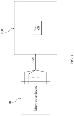
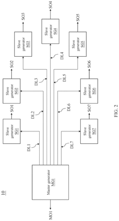
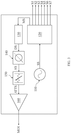
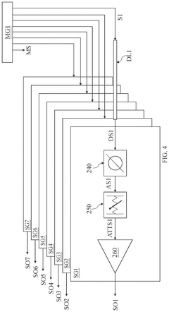
Microwave device
PatentPendingUS20250247926A1
Innovation
- A microwave device comprising a master generator, delay lines, and slave generators, where the master generator produces a source RF signal that is split and synchronized with slave generators through delay lines to achieve phase-coherent RF outputs, utilizing solid state microwave generators for improved control.
Thermal Management Strategies for Compact Designs
Effective thermal management is critical when optimizing magnetron packaging for reduced footprint. As magnetron components become more compact, heat dissipation challenges intensify due to increased power density within smaller volumes. Traditional cooling methods often prove inadequate for these high-density configurations, necessitating innovative thermal management approaches.
Heat generation in compact magnetrons primarily occurs at the anode and cathode interfaces, with temperatures potentially exceeding 200°C during operation. Without proper thermal management, these elevated temperatures can significantly reduce component lifespan, degrade performance, and potentially lead to catastrophic failures. The challenge is particularly acute in applications where space constraints limit the implementation of conventional cooling solutions.
Advanced materials with superior thermal conductivity properties represent a promising direction for compact magnetron designs. Ceramic-metal composites (cermets) and advanced copper alloys with enhanced thermal conductivity are being increasingly utilized as heat spreaders and thermal interfaces. These materials facilitate more efficient heat transfer from critical components to cooling structures while maintaining the electrical properties required for magnetron operation.
Active cooling technologies have evolved significantly to address compact magnetron requirements. Miniaturized liquid cooling systems using microchannels can remove heat more efficiently than traditional air cooling methods, offering up to 10 times greater heat flux dissipation. These systems can be integrated directly into the magnetron housing, minimizing the overall footprint while maximizing cooling efficiency.
Phase change materials (PCMs) present another innovative approach for thermal management in compact magnetrons. These materials absorb excess heat during peak operation by changing from solid to liquid state, effectively acting as thermal buffers. When integrated into magnetron packaging, PCMs can help maintain more consistent operating temperatures and reduce thermal cycling stress on components.
Computational fluid dynamics (CFD) modeling has become essential for optimizing thermal management in compact magnetron designs. These simulation tools enable engineers to predict hotspots, analyze airflow patterns, and evaluate cooling system performance before physical prototyping. Advanced thermal modeling can reduce development cycles by up to 40% while ensuring optimal thermal performance in the final design.
Integration of thermal sensors and adaptive cooling control systems represents the cutting edge of magnetron thermal management. These systems continuously monitor operating temperatures and adjust cooling parameters in real-time, optimizing performance while preventing thermal damage. Such intelligent thermal management systems can extend component lifespan by up to 30% while allowing for more aggressive miniaturization of magnetron packaging.
Manufacturing Processes for Optimized Packaging
The manufacturing processes for optimized magnetron packaging require innovative approaches to achieve reduced footprint while maintaining performance integrity. Advanced manufacturing techniques such as precision die-casting and automated assembly lines have revolutionized the production of compact magnetron units. These processes enable tighter tolerances and more precise component placement, critical factors in footprint reduction.
Surface-mount technology (SMT) has been adapted specifically for magnetron manufacturing, allowing for denser component placement and elimination of through-hole requirements that traditionally demanded more space. This adaptation has resulted in packaging size reductions of up to 30% compared to conventional manufacturing methods while maintaining thermal management capabilities.
Miniaturization-focused manufacturing processes incorporate multi-layer ceramic substrates that enable vertical integration of components. These substrates feature embedded passive components and optimized trace routing, significantly reducing the horizontal space requirements. The manufacturing process includes specialized high-temperature co-fired ceramic (HTCC) techniques that ensure structural integrity despite the reduced dimensions.
Precision micro-welding and laser bonding technologies have replaced bulkier mechanical fastening methods, eliminating the need for additional clearance space around connection points. These joining technologies maintain the necessary electromagnetic shielding properties while reducing the overall package dimensions by approximately 15-20% compared to traditional fastening methods.
Advanced cooling channel fabrication techniques have been developed specifically for compact magnetron designs. These include micro-channel cooling structures created through selective laser melting (SLM) and direct metal laser sintering (DMLS) processes. Such techniques allow for the integration of complex cooling geometries that would be impossible to manufacture using conventional methods, enabling more efficient heat dissipation in smaller packages.
Automated optical inspection (AOI) and X-ray inspection systems have been customized for quality control in compact magnetron manufacturing. These systems verify component placement accuracy to micron-level precision and ensure internal structural integrity without destructive testing. This capability is essential for maintaining reliability standards while pushing the boundaries of miniaturization.
Material innovations in manufacturing include the development of specialized composite materials with enhanced thermal conductivity and electromagnetic properties. These materials are processed using precision injection molding techniques that allow for thinner wall structures without compromising strength or shielding effectiveness, further contributing to footprint reduction goals.
Unlock deeper insights with Patsnap Eureka Quick Research — get a full tech report to explore trends and direct your research. Try now!
Generate Your Research Report Instantly with AI Agent
Supercharge your innovation with Patsnap Eureka AI Agent Platform!