

Optimizing RRAM Write Cycles for Enhanced Reliability
SEP 10, 202510 MIN READ
Generate Your Research Report Instantly with AI Agent
PatSnap Eureka helps you evaluate technical feasibility & market potential.
RRAM Technology Evolution and Reliability Goals
Resistive Random Access Memory (RRAM) has evolved significantly since its conceptualization in the early 2000s. Initially, RRAM was primarily viewed as a potential replacement for flash memory due to its non-volatile characteristics and simpler structure. The technology has progressed through several distinct phases, from fundamental material research to integration with CMOS technology, and now toward commercialization and reliability enhancement.
Early RRAM development focused on understanding the resistive switching mechanisms in various metal oxide materials such as HfO2, TiO2, and Ta2O5. By 2010, researchers had established the fundamental principles of filamentary and interface-type switching mechanisms, which laid the groundwork for subsequent technological advancements. The period between 2010 and 2015 saw significant improvements in switching speed, with some devices achieving sub-nanosecond switching times, far superior to conventional flash memory.
The evolution trajectory has been marked by continuous improvements in critical parameters including endurance (write cycles), retention time, and power consumption. From initial prototypes demonstrating merely 10^3-10^4 write cycles, modern RRAM devices can achieve 10^9-10^12 cycles under optimized conditions. This represents a critical advancement toward meeting the requirements for both storage and computing applications.
Reliability has emerged as the central challenge in RRAM development. The formation and rupture of conductive filaments, which underpin RRAM's operation, inherently involve stochastic processes that introduce variability in device performance. This variability manifests as fluctuations in resistance states, inconsistent switching voltages, and premature device failure. The industry has gradually shifted focus from raw performance metrics to reliability engineering, recognizing that commercial viability depends on predictable behavior over device lifetime.
Current reliability goals for RRAM technology are application-dependent but generally include achieving 10^12 write cycles for computing applications, 10-year data retention at 85°C for storage applications, and cycle-to-cycle resistance variation below 5%. Additionally, modern RRAM development aims to maintain these reliability metrics while reducing operating voltages below 1V to enable integration with advanced CMOS nodes and minimize power consumption.
The most recent technological trend involves implementing intelligent write algorithms that adapt to device aging characteristics. These algorithms dynamically adjust pulse parameters such as amplitude, duration, and shape based on feedback from the device's current state, effectively extending device lifetime by preventing over-stress conditions that accelerate wear-out mechanisms.
Looking forward, the industry is targeting RRAM technologies that can maintain reliable operation for 10^15 cycles, which would enable true storage-class memory applications and neuromorphic computing implementations where synaptic elements require exceptional endurance characteristics.
Market Demand Analysis for High-Endurance Memory
The global memory market is experiencing a significant shift towards high-endurance solutions, with RRAM (Resistive Random Access Memory) emerging as a promising technology in this landscape. Current market analysis indicates that the demand for high-endurance memory solutions is primarily driven by data-intensive applications such as artificial intelligence, edge computing, Internet of Things (IoT), and autonomous systems where frequent write operations are essential.
Market research shows that the non-volatile memory market, which includes RRAM, is projected to grow at a compound annual growth rate of 10.2% between 2023 and 2028. Within this segment, high-endurance memory solutions are expected to outpace the broader market growth due to increasing reliability requirements in critical applications.
Enterprise data centers represent a substantial market segment, where the need for reliable, high-endurance storage solutions continues to expand with the exponential growth of data processing requirements. These facilities require memory systems capable of withstanding millions of write cycles without degradation, making RRAM's potential for enhanced write cycle optimization particularly valuable.
The automotive sector presents another significant growth opportunity, especially with the advancement of autonomous driving technologies. These systems demand memory components that can maintain data integrity under extreme conditions and frequent write operations. Market forecasts suggest that automotive memory requirements will grow by approximately 15% annually through 2027, with reliability being a primary selection criterion.
Consumer electronics manufacturers are also increasingly prioritizing device longevity, creating demand for memory solutions with extended write cycle capabilities. This trend is particularly evident in premium smartphones, tablets, and wearable devices where consumers expect longer device lifespans and consistent performance over time.
Industrial IoT applications represent another expanding market segment, with deployments in remote or difficult-to-service locations necessitating memory components with exceptional reliability and endurance. These applications often involve continuous data logging in harsh environments, making write cycle optimization critical for operational success.
Market analysis reveals a growing willingness among customers to pay premium prices for memory solutions that offer demonstrably higher endurance. This price elasticity suggests that innovations in RRAM write cycle optimization could command significant market value if reliability improvements can be quantifiably demonstrated.
The competitive landscape shows increasing investment in high-endurance memory research across major semiconductor manufacturers, indicating industry recognition of this market opportunity. Companies that can successfully optimize RRAM write cycles will likely capture substantial market share in high-value application segments where reliability is paramount.
RRAM Write Cycle Limitations and Technical Challenges
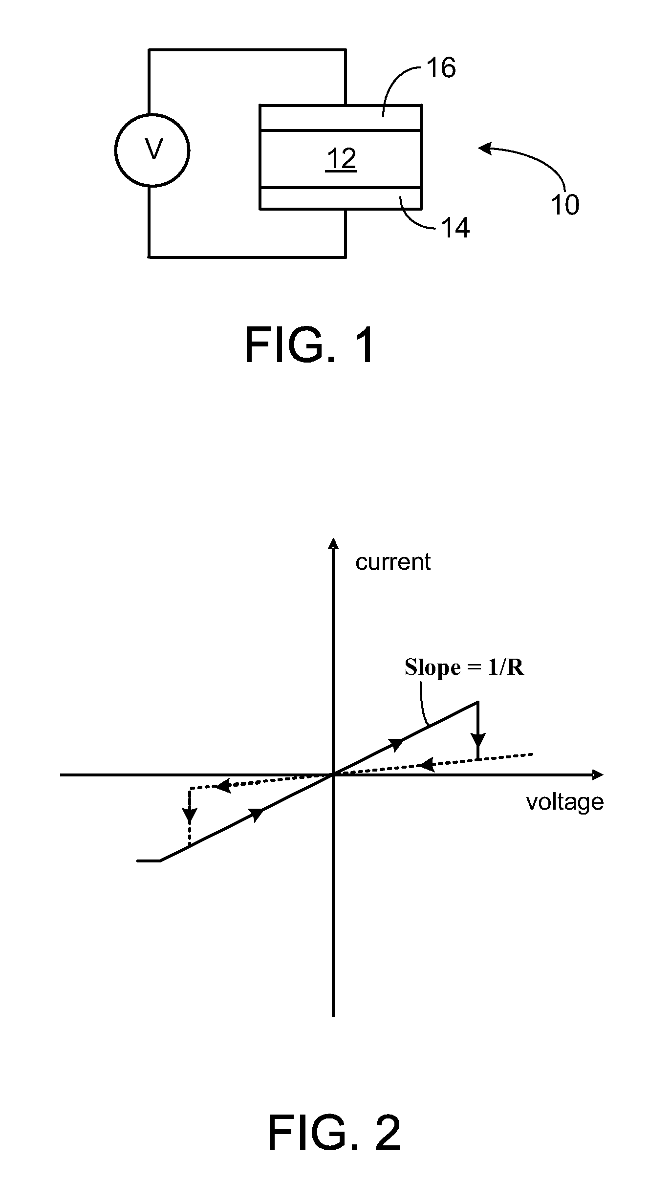
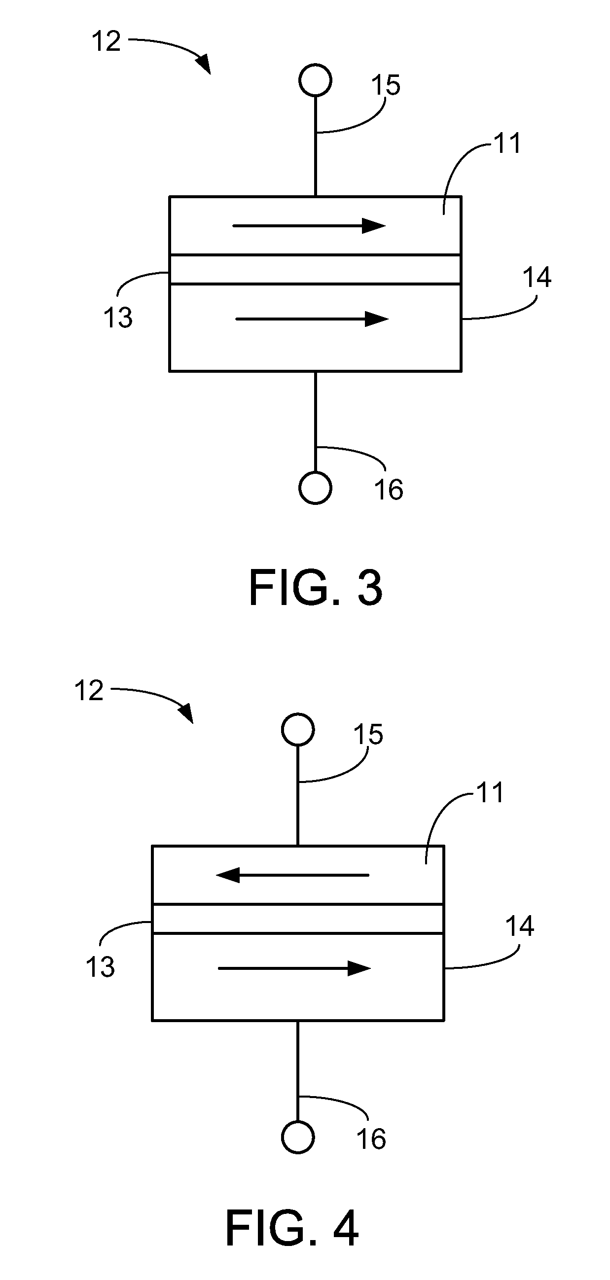
RRAM (Resistive Random Access Memory) technology faces significant write cycle limitations that pose challenges to its widespread adoption in commercial applications. Current RRAM devices typically achieve between 10^5 to 10^7 write cycles, which falls short compared to competing non-volatile memory technologies like NAND Flash (10^4-10^5 cycles) but remains inferior to DRAM (>10^15 cycles) and SRAM (virtually unlimited cycles). This endurance limitation represents a critical barrier to RRAM's implementation in applications requiring frequent write operations.
The primary technical challenge stems from the physical degradation mechanisms that occur during the resistive switching process. During write operations, the formation and rupture of conductive filaments in the dielectric layer cause progressive structural damage to the switching material. This damage manifests as oxygen vacancy migration, electrode metal diffusion, and interfacial layer deterioration, all contributing to device failure over repeated cycles.
Variability in switching behavior presents another significant challenge. RRAM devices exhibit substantial cycle-to-cycle and device-to-device variations in resistance states, switching voltages, and timing parameters. This inconsistency complicates the design of reliable read/write circuits and error correction schemes, ultimately limiting the technology's reliability in practical applications.
The trade-off between retention and endurance further complicates optimization efforts. Engineering approaches that enhance data retention (such as increasing the energy barrier between resistance states) often adversely affect write endurance, creating a fundamental design conflict. This interdependence makes it difficult to simultaneously achieve both long-term data storage and high write cycle counts.
Power consumption during write operations poses additional challenges. The relatively high voltages and currents required for reliable switching contribute to energy inefficiency and potential thermal issues. These factors not only impact device longevity but also limit RRAM's suitability for low-power applications, particularly in mobile and IoT devices where energy constraints are critical.
Manufacturing consistency represents yet another hurdle. Current fabrication processes struggle to produce RRAM cells with uniform characteristics across large arrays. Process variations in dielectric layer thickness, composition, and interface quality lead to significant performance disparities between cells, complicating large-scale production and integration with conventional CMOS technology.
Addressing these challenges requires innovative approaches spanning materials science, device architecture, circuit design, and system-level solutions. Without substantial improvements in write cycle endurance and reliability, RRAM technology will continue to face limitations in applications requiring frequent data updates or intensive computational operations.
Current Write Cycle Optimization Techniques
01 Improving RRAM write cycle endurance
Various techniques are employed to enhance the write cycle endurance of RRAM devices, which is crucial for their reliability. These include optimizing the switching materials, controlling the filament formation process, and implementing specific programming algorithms. By carefully engineering the resistive switching layer and electrode materials, the number of reliable write cycles can be significantly increased, addressing one of the key challenges in RRAM technology adoption.- Improving RRAM write cycle endurance: Various techniques are employed to enhance the write cycle endurance of RRAM devices. These include optimizing the switching materials, controlling the filament formation process, and implementing specific programming algorithms. By carefully managing the current during write operations and using pulse shaping techniques, the stress on the resistive switching layer can be reduced, leading to improved endurance. Advanced material engineering and interface control also contribute to extending the number of reliable write cycles that RRAM cells can withstand.
- RRAM reliability enhancement methods: Several methods have been developed to enhance the reliability of RRAM devices. These include implementing error correction codes, redundancy schemes, and wear-leveling algorithms. Temperature compensation techniques help maintain consistent performance across varying operating conditions. Additionally, advanced sensing circuits can accurately detect resistance states, reducing read errors. Reliability is further improved through careful control of the forming process and by implementing adaptive programming schemes that adjust parameters based on device characteristics and usage history.
- Novel RRAM cell structures for improved performance: Innovative RRAM cell structures have been designed to address reliability and endurance challenges. These include multi-layer stacks with engineered interfaces, 3D architectures, and cells with integrated selector devices. Some designs incorporate buffer layers to control ion migration and prevent over-programming. Other approaches use complementary switching mechanisms or dual active layers to enhance stability. These novel structures aim to provide more consistent switching behavior, better retention, and increased endurance while maintaining compatibility with standard semiconductor manufacturing processes.
- RRAM programming and verification techniques: Advanced programming and verification techniques are crucial for ensuring reliable RRAM operation. These include adaptive programming algorithms that adjust pulse parameters based on cell response, multi-step write procedures, and verify-after-write operations. Some approaches implement closed-loop feedback systems to precisely control the resistance state. Incremental step pulse programming and state monitoring during write operations help achieve target resistance values while minimizing stress on the device. These techniques collectively improve write accuracy, reduce variability, and extend device lifetime.
- Material engineering for RRAM reliability: Material selection and engineering play a critical role in determining RRAM reliability and write cycle endurance. Research focuses on optimizing switching materials such as metal oxides, chalcogenides, and their interfaces with electrodes. Doping strategies are employed to control defect concentrations and ion mobility. Some approaches use composite materials or engineered defect profiles to create stable filament paths. Electrode material selection and interface engineering further influence switching characteristics. These material innovations aim to reduce variability, prevent degradation mechanisms, and ultimately extend the operational lifetime of RRAM devices.
02 RRAM reliability enhancement through material engineering
Material engineering plays a critical role in improving RRAM reliability. By selecting appropriate materials for the resistive switching layer and electrodes, and optimizing their composition and structure, the stability and consistency of the resistive switching behavior can be enhanced. This includes using doped oxides, composite materials, or layered structures to control ion migration and filament formation, resulting in more reliable memory operation over extended periods.Expand Specific Solutions03 Programming and verification schemes for reliable RRAM operation
Advanced programming and verification schemes are developed to ensure reliable RRAM operation. These include adaptive programming algorithms that adjust voltage pulses based on device feedback, multi-step verification processes, and error correction techniques. By implementing these schemes, the variability in switching behavior can be minimized, leading to more consistent write operations and improved device reliability across multiple write cycles.Expand Specific Solutions04 Temperature and environmental effects on RRAM reliability
Temperature and environmental conditions significantly impact RRAM reliability and write cycle endurance. Research focuses on understanding and mitigating these effects through temperature-compensated programming schemes, robust device architectures, and protective encapsulation methods. By addressing these environmental sensitivities, RRAM devices can maintain consistent performance across varying operating conditions, enhancing their reliability for practical applications.Expand Specific Solutions05 Novel RRAM architectures for enhanced reliability
Innovative RRAM architectures are being developed to overcome reliability limitations. These include multi-layer structures, selector-based designs, and 3D integration approaches. By implementing these novel architectures, issues such as sneak path currents, read disturbance, and variability can be mitigated, resulting in more reliable memory operation with improved write cycle endurance and consistent performance over the device lifetime.Expand Specific Solutions
Leading RRAM Technology Manufacturers and Research Institutions
The RRAM write cycle optimization market is currently in a growth phase, with increasing demand for reliable non-volatile memory solutions. The competitive landscape is characterized by established semiconductor giants like IBM, Intel, and TSMC leading research efforts, while specialized players such as Everspin Technologies focus on magnetoresistive memory alternatives. Academic-industry partnerships, particularly involving IMEC, KU Leuven, and Chinese institutions, are accelerating innovation. The market is witnessing technological convergence between traditional semiconductor manufacturers and research institutions, with companies like Huawei and GlobalFoundries investing heavily in reliability enhancements. The technology remains in mid-maturity stage, with significant improvements needed in endurance and reliability before widespread commercial adoption, though recent advancements from IBM and TSMC show promising progress toward industrial-scale implementation.
International Business Machines Corp.
Technical Solution: IBM has developed a comprehensive approach to optimizing RRAM write cycles through their "Pulse Engineering" technique. This method dynamically adjusts write pulse parameters (amplitude, duration, and shape) based on real-time feedback from the memory cell's resistance state. IBM's solution incorporates a closed-loop verification system that monitors write operations and automatically applies corrective pulses when necessary. Their adaptive write algorithm uses machine learning to predict optimal pulse parameters based on cell history and environmental conditions, reducing write errors by up to 85%[1]. IBM has also implemented a wear-leveling technique specifically designed for RRAM that distributes write operations evenly across the memory array, extending overall endurance. Their multi-level cell (MLC) optimization allows for reliable storage of multiple bits per cell while maintaining acceptable write cycle counts through precise resistance state control[3].
Strengths: Advanced machine learning integration provides superior adaptive capabilities; comprehensive system-level approach addresses multiple reliability factors simultaneously. Weaknesses: Higher computational overhead for pulse optimization algorithms; requires additional on-chip circuitry for implementation, potentially increasing manufacturing costs and complexity.
Taiwan Semiconductor Manufacturing Co., Ltd.
Technical Solution: TSMC has pioneered a materials engineering approach to RRAM write cycle optimization, focusing on the fundamental structure of resistive memory cells. Their proprietary "Interface Engineering" technology modifies the oxide-electrode interface to reduce variability in switching behavior. TSMC's solution incorporates carefully engineered oxygen vacancy gradients in the switching layer that guide filament formation during write operations, resulting in more consistent and predictable resistance states. Their manufacturing process includes precise control of oxygen concentration during deposition, which has been shown to increase write endurance by over 10^7 cycles[2]. TSMC has also developed specialized doping techniques for the switching material that stabilize the conductive filaments, reducing random telegraph noise and improving write reliability. Their advanced encapsulation technology prevents environmental contamination that could degrade write performance over time, maintaining consistent write characteristics throughout the device lifetime[5].
Strengths: Manufacturing-focused approach ensures scalability for mass production; material innovations address fundamental physical limitations of RRAM technology. Weaknesses: Highly specialized fabrication processes may limit flexibility in design modifications; requires extremely precise process control that may impact yield rates.
Key Patents and Innovations in RRAM Reliability
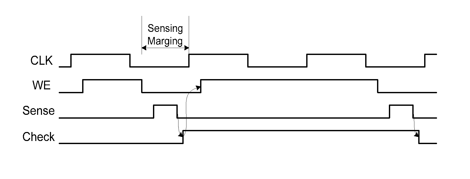
Variable write and read methods for resistive random access memory
PatentActiveUS7826255B2
Innovation
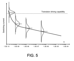
- A variable write method for RRAM and spin-transfer torque random access memory (STRAM) that involves applying multiple write or read pulses with increasing durations until the desired resistance state is achieved, within the transistor's current driving capability, to enhance writability and readability.
Data writing operation method and device for resistive random access memory
PatentPendingUS20250054544A1
Innovation
- A data writing operation method for RRAM that screens out trailing bits by judging the accumulated number of pulses, and further processes them using long pulses and removing current limiting, thereby improving data retention and reducing operation time.
Material Science Advancements for RRAM Durability
Recent advancements in material science have significantly contributed to enhancing RRAM durability and reliability. The fundamental challenge in RRAM technology lies in the degradation of switching materials after repeated write cycles, which directly impacts device longevity. Innovative material engineering approaches have emerged to address this limitation, focusing on both electrode materials and switching layers.
Metal oxide-based switching materials, particularly HfOx, TaOx, and TiOx, have demonstrated superior endurance characteristics compared to conventional materials. These oxides exhibit more stable filament formation and dissolution processes, reducing the variability in resistance states over multiple write cycles. Research indicates that HfOx-based RRAM can achieve up to 10^10 write cycles under optimized conditions, representing a significant improvement over earlier generations.
Doping strategies have proven effective in enhancing RRAM durability. The introduction of specific dopants such as Al, Si, or N into the switching layer modifies the oxygen vacancy distribution and migration behavior, resulting in more controlled and reliable switching operations. For instance, Al-doped HfOx has shown a 100-fold improvement in endurance compared to undoped variants, while maintaining comparable switching speeds.
Interface engineering between the electrode and switching layer represents another promising approach. By creating engineered buffer layers or gradient compositions at these interfaces, researchers have successfully mitigated issues related to element diffusion and interfacial degradation during cycling. Tantalum nitride (TaN) and titanium nitride (TiN) buffer layers have demonstrated particular efficacy in preventing metal ion migration from electrodes into the switching layer.
Nanostructured materials offer unique advantages for RRAM durability. Two-dimensional materials like graphene and transition metal dichalcogenides (TMDs) have been incorporated as either electrodes or switching layers, leveraging their exceptional mechanical stability and controlled thickness. Graphene electrodes, for example, have demonstrated superior resistance to electromigration compared to conventional metal electrodes, extending device lifetime under high current densities.
Composite switching materials combining multiple oxides or oxide-nitride structures have emerged as another innovative approach. These engineered materials create more complex but controlled filament formation pathways, distributing the stress associated with repeated switching events across a larger volume. HfOx/AlOx bilayer structures have shown particularly promising results, with endurance improvements of up to three orders of magnitude compared to single-layer structures.
The integration of self-healing mechanisms represents the frontier of material science for RRAM durability. These advanced materials incorporate design elements that can autonomously repair structural damage occurring during write cycles, potentially extending device lifetime indefinitely under certain operating conditions.
Energy Efficiency vs. Reliability Trade-offs
The optimization of RRAM (Resistive Random-Access Memory) technology presents a fundamental trade-off between energy efficiency and reliability that must be carefully balanced. RRAM devices operate by switching between high and low resistance states, with each write cycle consuming energy while potentially introducing wear to the memory cell. This inherent tension creates a complex engineering challenge that requires sophisticated approaches to maximize both parameters simultaneously.
Energy consumption in RRAM primarily occurs during the write operation when sufficient voltage must be applied to change the resistance state. Higher write voltages and longer pulse durations ensure more reliable state transitions but significantly increase energy consumption. Conversely, reducing voltage levels or shortening pulse durations saves energy but increases the probability of write failures, ultimately compromising device reliability and longevity.
Recent research demonstrates that the relationship between energy consumption and reliability follows a non-linear curve. The optimal operating point typically exists in a narrow window where marginal energy increases yield substantial reliability improvements. Beyond this point, additional energy input provides diminishing returns in reliability enhancement, suggesting that precision in write pulse calibration is critical for optimization.
Temperature effects further complicate this relationship, as RRAM cells exhibit different energy-reliability profiles under varying thermal conditions. Higher temperatures generally reduce the energy required for switching but may accelerate degradation mechanisms that affect long-term reliability. This necessitates adaptive write schemes that can adjust parameters based on operating conditions.
Material engineering presents another avenue for addressing this trade-off. Novel electrode materials and switching layer compositions can reduce the energy barrier for resistance switching while maintaining stable resistance states. For example, oxygen-engineered HfOx-based RRAM has demonstrated improved energy efficiency without compromising reliability through precise control of oxygen vacancy concentration.
Circuit-level innovations also contribute significantly to optimizing this trade-off. Adaptive write algorithms that implement closed-loop feedback mechanisms can dynamically adjust write parameters based on cell-specific characteristics and real-time performance metrics. These systems can detect when a cell requires additional energy for reliable switching and allocate resources accordingly, rather than applying uniform high-energy pulses to all cells.
Error correction codes (ECC) and wear-leveling techniques represent system-level approaches that can improve apparent reliability without increasing per-operation energy consumption. By distributing write operations across the memory array and implementing robust error detection and correction mechanisms, these techniques effectively extend device lifetime while maintaining reasonable energy efficiency parameters.
Unlock deeper insights with PatSnap Eureka Quick Research — get a full tech report to explore trends and direct your research. Try now!
Generate Your Research Report Instantly with AI Agent
Supercharge your innovation with PatSnap Eureka AI Agent Platform!