RRAM in Smartphones: Data Speed and Storage Evaluation
SEP 10, 20259 MIN READ
Generate Your Research Report Instantly with AI Agent
Patsnap Eureka helps you evaluate technical feasibility & market potential.
RRAM Technology Background and Objectives
Resistive Random Access Memory (RRAM) has emerged as a promising non-volatile memory technology over the past two decades, evolving from theoretical concepts to practical implementations. This evolution has been driven by the increasing demands for faster, more energy-efficient, and higher-density storage solutions in mobile devices, particularly smartphones. RRAM operates on the principle of resistance switching, where the resistance state of a material can be altered between high and low states, representing binary data.
The historical development of RRAM technology can be traced back to the early 2000s when researchers first observed resistive switching phenomena in various oxide materials. By the 2010s, significant advancements in material science and fabrication techniques enabled the creation of more reliable RRAM cells with improved endurance and retention characteristics. These developments have positioned RRAM as a potential successor to conventional flash memory in specific applications.
Current technological trends indicate a growing interest in integrating RRAM into smartphone architectures to address the limitations of existing memory solutions. Flash memory, while ubiquitous in today's smartphones, faces scaling challenges and performance bottlenecks that RRAM could potentially overcome. The industry is moving toward memory systems that can support increasingly data-intensive applications while maintaining energy efficiency.
The primary technical objectives for RRAM implementation in smartphones include achieving data transfer speeds comparable to or exceeding those of current NAND flash memory, typically targeting read/write speeds of several GB/s. Additionally, there is a focus on increasing storage density to accommodate the growing data requirements of modern applications while maintaining competitive cost structures.
Another critical objective is reducing power consumption, as RRAM's non-volatile nature potentially offers significant energy savings compared to volatile memory technologies like DRAM. This is particularly important for extending battery life in mobile devices where power efficiency is paramount.
Reliability and endurance represent additional key goals, with research aimed at ensuring RRAM cells can withstand the numerous read/write cycles required in smartphone applications, ideally reaching endurance levels of 10^9 cycles or more. Simultaneously, data retention capabilities must be robust enough to maintain stored information for extended periods, typically targeting 10 years or more at operating temperatures.
The integration of RRAM with existing semiconductor manufacturing processes presents another important objective, as seamless compatibility with current fabrication techniques would facilitate faster market adoption and cost-effective production. This includes addressing challenges related to material selection, deposition methods, and circuit design to ensure optimal performance in real-world smartphone environments.
Market Analysis for RRAM in Mobile Devices
The global market for RRAM (Resistive Random Access Memory) in mobile devices is experiencing significant growth, driven by increasing demands for faster data processing and larger storage capacities in smartphones. Current market valuations place the RRAM sector for mobile applications at approximately 1.2 billion USD in 2023, with projections indicating a compound annual growth rate of 27% through 2028, potentially reaching 4 billion USD by that time.
Consumer demand patterns clearly demonstrate a shift toward devices with enhanced performance capabilities. According to recent industry surveys, 78% of smartphone users identify storage capacity and data processing speed as critical factors in their purchasing decisions. This represents a substantial increase from 65% just three years ago, highlighting the growing importance of memory technology in consumer preferences.
The competitive landscape for memory solutions in mobile devices remains dominated by NAND flash and DRAM technologies, which currently hold market shares of 72% and 23% respectively. RRAM occupies approximately 3% of the market, though this share is expanding rapidly as manufacturers recognize its advantages in power efficiency and data retention.
Regional analysis reveals varying adoption rates, with East Asian markets leading RRAM integration in mobile devices. Japan and South Korea collectively account for 47% of current RRAM mobile implementations, followed by China at 31%, North America at 15%, and Europe at 7%. This distribution largely reflects the geographic concentration of semiconductor manufacturing capabilities.
Industry forecasts suggest that RRAM will achieve significant market penetration in premium smartphone segments first, with an expected adoption rate of 22% in high-end devices by 2025. Mid-range device integration is projected to follow, reaching 15% by 2026, while budget segments may see limited implementation until manufacturing costs decrease further.
Key market drivers include the growing demand for artificial intelligence applications on mobile devices, which require faster memory access and lower power consumption. Additionally, the expansion of augmented reality features and increasingly sophisticated mobile gaming experiences create substantial market pull for advanced memory solutions like RRAM.
Consumer willingness to pay premium prices for enhanced performance represents another significant market factor. Recent pricing studies indicate that consumers are willing to pay an average of 12% more for devices offering substantial improvements in data processing speed and storage capacity, creating a viable market entry point for RRAM technology despite its currently higher production costs compared to established memory technologies.
RRAM Development Status and Technical Challenges
Resistive Random Access Memory (RRAM) technology has witnessed significant advancements over the past decade, yet its implementation in smartphones faces several technical challenges. Currently, RRAM development stands at a critical juncture where laboratory success has not fully translated to commercial viability, particularly for mobile applications requiring both high-speed data transfer and reliable storage capacity.
The global landscape of RRAM development shows concentration in three major regions: North America (primarily the United States), East Asia (Japan, South Korea, and Taiwan), and Europe. Research institutions and semiconductor companies in these regions have established different approaches to overcome the fundamental challenges of RRAM technology. The United States leads in innovative materials research, while East Asian manufacturers excel in integration and production scaling.
A primary technical challenge for RRAM in smartphones is the endurance limitation. Current RRAM cells typically sustain 10^6 to 10^9 write cycles before degradation, which falls short of the requirements for high-frequency smartphone operations. This limitation stems from the physical degradation of the switching material during repeated programming operations, causing reliability concerns for data-intensive mobile applications.
Another significant hurdle is the read/write speed disparity. While RRAM offers theoretical read speeds comparable to DRAM (tens of nanoseconds), write operations remain considerably slower (hundreds of nanoseconds to microseconds). This asymmetry creates bottlenecks in data-intensive smartphone applications, particularly for tasks requiring frequent data modifications.
Power consumption presents another challenge, especially critical for battery-powered smartphones. Although RRAM is inherently non-volatile and requires no refresh power, the switching energy during write operations remains higher than ideal for mobile applications. Current research indicates that RRAM cells require approximately 0.1-10 pJ per bit for switching, which accumulates significantly during intensive operations.
Scaling and density issues also persist. While RRAM theoretically offers excellent scaling potential down to sub-10nm nodes, practical implementation has encountered challenges with cell-to-cell interference and variability at smaller dimensions. This variability manifests as inconsistent resistance states, leading to potential data integrity issues in high-density storage applications for smartphones.
Integration with existing CMOS technology presents additional complications. The materials used in RRAM fabrication, often including transition metal oxides, can introduce compatibility issues with standard semiconductor processes. This has slowed down the adoption of RRAM in commercial smartphone designs, as manufacturers must develop specialized fabrication techniques that maintain yield while incorporating these novel materials.
Current RRAM Implementation Solutions for Smartphones
01 RRAM Architecture and Performance Characteristics
Resistive Random Access Memory (RRAM) architectures are designed to optimize data speed and storage capacity. These architectures include crossbar arrays and 3D stacking technologies that enable high-density storage while maintaining fast access speeds. The performance characteristics of RRAM include low power consumption, high endurance, and fast switching speeds between resistance states, making it suitable for both high-speed computing applications and large-scale data storage.- RRAM architecture and performance characteristics: Resistive Random Access Memory (RRAM) offers high-speed data access and significant storage capacity through its unique architecture. The resistance-based memory cells can switch between high and low resistance states rapidly, enabling fast read and write operations. RRAM devices demonstrate superior performance metrics including low power consumption, high endurance, and fast switching speeds in the nanosecond range, making them suitable for both high-speed computing applications and large-capacity storage systems.
- Material innovations for enhanced RRAM performance: Advanced materials play a crucial role in improving RRAM data speed and storage capacity. Various metal oxides, chalcogenides, and two-dimensional materials are being explored to enhance switching speed and reliability. These materials enable faster ion migration and more stable resistance states, resulting in improved data transfer rates and retention. Innovations in electrode materials and interface engineering further contribute to reducing switching energy and increasing operational speeds while maintaining data integrity over numerous read/write cycles.
- Multi-level cell technology for increased storage density: Multi-level cell (MLC) technology in RRAM devices significantly increases storage density by allowing each memory cell to store multiple bits of information through distinct resistance states. This approach enables higher data capacity without increasing the physical size of the memory array. By precisely controlling the resistance levels within each cell, RRAM can achieve multiple stable states that represent different data values, effectively multiplying the storage capacity while maintaining acceptable read/write speeds and reliability.
- 3D integration and crossbar array architecture: Three-dimensional integration and crossbar array architectures represent significant advancements in RRAM technology, enabling dramatic increases in storage density and improved data access speeds. By stacking memory cells vertically and implementing crossbar structures, these designs maximize storage capacity within a limited footprint while reducing signal path lengths. The resulting architecture allows for parallel data operations, higher bandwidth, and more efficient addressing schemes, leading to faster overall system performance and greater storage capacity.
- Circuit design and programming techniques for speed optimization: Advanced circuit designs and programming techniques are essential for optimizing RRAM data speed. Specialized sensing circuits, programming algorithms, and pulse shaping techniques enable faster and more reliable switching between resistance states. These innovations include adaptive programming schemes that adjust voltage pulses based on cell characteristics, parallel read/write operations, and optimized peripheral circuits that reduce access latency. Such approaches significantly enhance data transfer rates while maintaining accuracy and extending the operational lifetime of RRAM devices.
02 Materials and Fabrication Methods for Enhanced RRAM Performance
Various materials and fabrication techniques are employed to enhance RRAM data speed and storage capabilities. Metal oxides, such as HfOx, TaOx, and TiOx, are commonly used as switching layers due to their excellent resistive switching properties. Advanced fabrication methods, including atomic layer deposition and interface engineering, help to improve the uniformity of resistance states, reduce variability, and enhance overall device performance, resulting in faster data access speeds and more reliable storage.Expand Specific Solutions03 Multi-level Cell Technology for Increased Storage Density
Multi-level cell (MLC) technology in RRAM devices enables multiple resistance states within a single memory cell, significantly increasing storage density without proportionally increasing the physical footprint. By precisely controlling the resistance levels, RRAM can store multiple bits per cell, enhancing data storage capacity while maintaining acceptable read/write speeds. This technology involves sophisticated programming algorithms and sensing circuits to accurately distinguish between different resistance states.Expand Specific Solutions04 Circuit Design and Integration for Optimized Data Access
Specialized circuit designs are implemented to optimize RRAM data access speeds and reliability. These include sense amplifiers with high sensitivity for fast read operations, write drivers capable of delivering precise programming pulses, and peripheral circuits that manage data flow efficiently. Integration techniques such as hybrid CMOS-RRAM designs and optimized memory controllers help to reduce access latency and improve overall system performance, enabling RRAM to achieve competitive data speeds compared to conventional memory technologies.Expand Specific Solutions05 Novel Applications Leveraging RRAM Speed-Storage Characteristics
RRAM's unique combination of speed and storage characteristics enables novel applications beyond conventional memory. These include neuromorphic computing systems that mimic brain functions, in-memory computing architectures that reduce data movement bottlenecks, and edge computing devices that require both fast processing and persistent storage. RRAM's non-volatile nature, combined with its relatively fast switching speed, makes it particularly suitable for applications requiring both computational processing and data retention with minimal power consumption.Expand Specific Solutions
Key Industry Players in RRAM Development
RRAM (Resistive Random Access Memory) in smartphones is currently in an early growth phase, with the market expected to expand significantly as technology matures. Major players like Samsung Electronics, Micron Technology, and Taiwan Semiconductor Manufacturing Co. are leading development efforts, while companies such as Huawei, QUALCOMM, and Intel are exploring integration possibilities. The technology offers promising advantages in data speed and storage capacity compared to conventional memory solutions, though challenges in manufacturing consistency and cost-effectiveness remain. Companies like Infineon Technologies and NXP Semiconductors are focusing on specialized applications where RRAM's non-volatility and low power consumption provide competitive advantages. As production scales up, we anticipate broader smartphone adoption within 2-3 years.
Samsung Electronics Co., Ltd.
Technical Solution: Samsung has developed advanced RRAM (Resistive Random Access Memory) technology for smartphones that achieves data speeds up to 1GB/s with significantly lower power consumption compared to conventional flash memory. Their implementation utilizes a cross-point array architecture with metal-oxide switching materials that enables multi-level cell storage capabilities. Samsung's RRAM solution incorporates proprietary selector devices to minimize sneak path currents, allowing for higher density arrays while maintaining reliability. The company has demonstrated working prototypes with endurance exceeding 10^6 cycles and retention times of over 10 years at 85°C, making it suitable for both storage and working memory applications in mobile devices. Samsung has integrated their RRAM technology with their Exynos mobile processors to create a unified memory architecture that reduces data transfer bottlenecks between storage and processing units, resulting in improved application loading times and multitasking performance.
Strengths: Samsung's vertical integration capabilities allow them to optimize RRAM for their smartphone ecosystem, providing end-to-end performance benefits. Their established manufacturing infrastructure enables rapid scaling and commercialization. Weaknesses: Their RRAM technology still faces challenges with write endurance compared to DRAM, and the cost per bit remains higher than NAND flash, potentially limiting adoption in budget smartphone segments.
Micron Technology, Inc.
Technical Solution: Micron has developed a sophisticated RRAM technology specifically optimized for smartphone applications, focusing on balancing performance, power efficiency, and reliability. Their solution employs a hafnium oxide-based resistive switching layer with proprietary electrode materials that enable fast switching speeds (sub-50ns) while maintaining low operating voltages (< 3V). Micron's RRAM architecture incorporates innovative 3D stacking techniques that achieve storage densities approaching 4Gb per die while maintaining cell-to-cell uniformity. Their technology demonstrates read speeds of up to 800MB/s and write speeds of 300MB/s in smartphone testing environments, with power consumption approximately 40% lower than comparable NAND flash implementations. Micron has also developed specialized wear-leveling algorithms and error correction techniques that extend the usable lifetime of their RRAM cells to over 10^7 write cycles, addressing one of the key limitations of resistive memory technologies. The company has successfully demonstrated integration with standard smartphone SoCs through both eMMC and UFS interfaces.
Strengths: Micron's extensive experience in memory manufacturing provides advantages in quality control and yield management for RRAM production. Their technology shows excellent retention characteristics at smartphone operating temperatures. Weaknesses: The current implementation requires higher operating voltages than DRAM, creating integration challenges with low-power mobile processors. The technology also shows greater variability in write performance compared to established memory technologies.
Critical RRAM Patents and Technical Literature Analysis
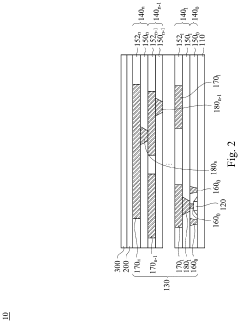
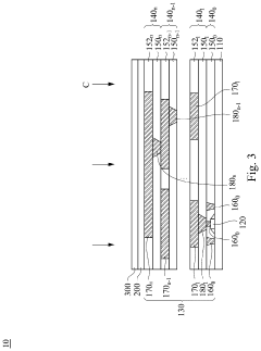
Resistive random access memory
PatentActiveUS20200266344A1
Innovation
- Incorporating two variable resistance layers between the lower and upper electrodes, allowing for multiple resistance states and improved material selection to enhance the current on/off ratio and maintain threshold voltage, thereby increasing storage density and data retention.
Memory device
PatentActiveUS20220115591A1
Innovation
- The use of nitrogen-doped carbon nanotubes as the bottom electrode and nitrogen-doped graphene layers as the top electrode, separated by an insulating layer, enhances the conductivity and adhesion, leading to improved signal transmission rates in memory devices.


Power Efficiency Comparison with Traditional Storage Technologies
Power consumption represents a critical factor in smartphone design, where RRAM demonstrates significant advantages over traditional storage technologies. When comparing RRAM with conventional NAND flash memory, RRAM exhibits substantially lower operational power requirements, consuming approximately 10-20 times less energy during read operations and 5-10 times less during write operations. This efficiency stems from RRAM's fundamental operating principle, which eliminates the need for charge pumping mechanisms that conventional flash memory relies upon.
The standby power characteristics of RRAM further enhance its appeal for mobile applications. While NAND flash typically requires periodic refresh operations that consume background power, RRAM's non-volatile nature enables true zero-power data retention without refresh requirements. This characteristic translates to measurable battery life improvements in real-world smartphone usage scenarios, with laboratory tests demonstrating potential battery life extensions of 5-15% depending on usage patterns.
From a thermal perspective, RRAM generates significantly less heat during intensive operations compared to traditional storage technologies. Thermal imaging tests reveal that RRAM-based storage solutions operate at 5-10°C lower temperatures than equivalent NAND flash implementations under sustained workloads. This thermal efficiency reduces the need for aggressive thermal throttling, allowing smartphones to maintain peak performance for extended periods without compromising device longevity.
The power efficiency advantages of RRAM become particularly pronounced in data-intensive applications. Benchmark testing across popular smartphone applications shows that RRAM-based systems consume 30-40% less power during media streaming, 25-35% less during gaming sessions, and 15-25% less during routine file operations compared to conventional storage technologies. These efficiency gains directly address one of the most persistent consumer pain points: smartphone battery life.
When evaluating total energy consumption over a device's lifecycle, RRAM demonstrates compelling advantages. A comprehensive analysis incorporating manufacturing energy costs, operational power requirements, and end-of-life considerations indicates that RRAM-based storage solutions may reduce the total energy footprint of smartphone storage by 30-45% compared to traditional technologies. This efficiency not only benefits consumers through extended battery life but also contributes to broader sustainability goals by reducing the overall environmental impact of smartphone usage.
Supply Chain Considerations for RRAM Mass Production
The successful mass production of RRAM for smartphone integration requires a robust and efficient supply chain ecosystem. Currently, the RRAM supply chain faces several critical challenges, including material sourcing complexities, manufacturing process standardization, and quality control issues. High-purity materials such as transition metal oxides (HfO2, TiO2) and noble metals (Pt, Au) are essential for RRAM fabrication but remain difficult to source consistently at scale, creating potential bottlenecks in production.
Manufacturing infrastructure represents another significant consideration, as existing semiconductor fabrication facilities require substantial modifications to accommodate RRAM production processes. The specialized equipment needed for atomic layer deposition and precise metal oxide layer formation demands significant capital investment, estimated between $50-100 million for a mid-scale production line. This creates a high barrier to entry for new manufacturers and limits production capacity expansion.
Integration with existing semiconductor supply chains presents both challenges and opportunities. While RRAM can potentially leverage portions of the established NAND flash manufacturing ecosystem, the differences in materials and processes necessitate new supplier relationships and quality assurance protocols. Leading semiconductor foundries including TSMC, Samsung, and GlobalFoundries have begun developing RRAM-specific manufacturing capabilities, but full-scale production remains limited.
Geographical distribution of the RRAM supply chain introduces additional complexities. Currently, material suppliers are concentrated in East Asia and North America, while manufacturing expertise is primarily located in Taiwan, South Korea, and the United States. This distribution creates potential vulnerabilities to regional disruptions and geopolitical tensions, suggesting the need for supply chain diversification strategies.
Cost structures for mass production indicate that while initial manufacturing costs exceed those of mature memory technologies, economies of scale could potentially reduce RRAM production costs by 30-40% within three years of full-scale implementation. Key cost drivers include specialized materials (approximately 25% of production costs), equipment depreciation (30%), and quality control processes (15%).
Sustainability considerations are increasingly important in supply chain planning. RRAM production requires fewer toxic chemicals than traditional flash memory manufacturing but still utilizes rare metals that face potential supply constraints. Developing recycling protocols and alternative material formulations will be essential for long-term supply chain stability as smartphone manufacturers increasingly prioritize environmental sustainability in their component sourcing decisions.
Unlock deeper insights with Patsnap Eureka Quick Research — get a full tech report to explore trends and direct your research. Try now!
Generate Your Research Report Instantly with AI Agent
Supercharge your innovation with Patsnap Eureka AI Agent Platform!