RRAM vs 3D NAND: Assessing Storage Capacity & Speed
SEP 10, 20259 MIN READ
Generate Your Research Report Instantly with AI Agent
Patsnap Eureka helps you evaluate technical feasibility & market potential.
RRAM and 3D NAND Evolution and Objectives
Memory technologies have undergone significant evolution over the past decades, with RRAM (Resistive Random Access Memory) and 3D NAND representing two distinct approaches to addressing growing storage demands. RRAM emerged in the early 2000s as a promising non-volatile memory technology based on resistance switching mechanisms. Its development was driven by the need for faster, more energy-efficient alternatives to traditional flash memory, with potential applications in both storage and computing.
3D NAND, meanwhile, represents the three-dimensional evolution of traditional NAND flash memory. First commercialized by Samsung in 2013 with its V-NAND technology, 3D NAND addressed the scaling limitations of planar NAND by stacking memory cells vertically. This architectural innovation has enabled continuous capacity increases while maintaining cost efficiency, becoming the dominant technology in today's solid-state storage market.
The technological trajectories of these memory technologies reflect broader industry trends toward higher density, improved performance, and reduced power consumption. RRAM development has focused on materials science innovations, exploring various metal oxides and switching mechanisms to optimize reliability and endurance. Concurrently, 3D NAND has progressed through increasing layer counts, from early 24-layer designs to current products exceeding 200 layers.
Market forces have shaped these evolutionary paths differently. 3D NAND has benefited from massive industry investment due to immediate commercial applications in consumer and enterprise storage. RRAM, despite its theoretical advantages, has faced challenges in scaling production and achieving cost parity with established technologies, resulting in a more specialized development trajectory focused on niche applications.
The primary technical objectives for both technologies center on addressing the storage-performance gap in computing architectures. For RRAM, objectives include achieving higher density while maintaining its inherent speed advantages, improving endurance cycles, and reducing manufacturing complexity. For 3D NAND, key goals involve continuing vertical scaling beyond current layer counts, improving read/write speeds, and enhancing reliability at smaller process nodes.
Looking forward, both technologies aim to support emerging computational paradigms. RRAM shows particular promise for in-memory computing and neuromorphic applications, where its resistance-based operation aligns well with neural network implementations. 3D NAND development increasingly focuses on supporting workload-specific optimizations and meeting the demands of AI and big data applications through architectural innovations like zoned namespaces and computational storage.
Storage Market Demand Analysis
The global storage market is experiencing unprecedented growth, driven by the explosion of data generation across various sectors. Current estimates place the data storage market at approximately $78 billion in 2023, with projections indicating growth to reach $118 billion by 2028, representing a compound annual growth rate (CAGR) of 8.6%. This expansion is primarily fueled by the increasing adoption of cloud services, big data analytics, artificial intelligence applications, and the proliferation of connected devices in the Internet of Things (IoT) ecosystem.
Within this expanding market, there is a growing demand for storage solutions that offer higher capacity, improved speed, and enhanced energy efficiency. Traditional storage technologies are struggling to keep pace with these requirements, creating significant market opportunities for emerging technologies like RRAM (Resistive Random-Access Memory) and advanced 3D NAND architectures.
Enterprise storage demands are shifting dramatically, with organizations requiring solutions capable of handling real-time data processing and analysis. According to industry surveys, approximately 67% of enterprise customers identify storage speed as a critical factor in their purchasing decisions, while 82% emphasize the importance of storage capacity. This dual requirement creates a complex market landscape where technologies must balance these sometimes competing priorities.
The consumer electronics segment represents another substantial market driver, with smartphones, tablets, and laptops requiring increasingly sophisticated storage solutions. Market research indicates that consumers are willing to pay premium prices for devices offering faster data access and greater storage capacity, with 73% of smartphone buyers considering storage specifications as a key purchase criterion.
Edge computing applications are emerging as a particularly promising market segment for next-generation storage technologies. As computational workloads move closer to data sources, the demand for high-performance, energy-efficient storage at the network edge is growing at 24% annually, significantly outpacing the broader storage market.
Regionally, North America currently dominates the advanced storage market with approximately 38% market share, followed by Asia-Pacific at 34%, which is experiencing the fastest growth rate. The European market accounts for 22% of global demand, with particular strength in industrial and automotive applications.
Market forecasts suggest that technologies offering substantial improvements in both capacity and speed metrics will capture premium market segments, with potential price premiums of 30-45% over conventional solutions. This creates a compelling business case for continued investment in advanced storage technologies like RRAM and enhanced 3D NAND architectures.
Technical Challenges in Memory Technologies
Memory technologies face several significant technical challenges that impact their performance, scalability, and commercial viability. For RRAM (Resistive Random Access Memory) and 3D NAND, these challenges manifest in distinct ways that affect their storage capacity and speed capabilities.
RRAM confronts material stability issues that directly impact its reliability and endurance. The resistance switching mechanism, while promising for high-density storage, suffers from variability in switching behavior across multiple cycles. This inconsistency creates challenges in maintaining stable resistance states, leading to potential data retention problems and limiting practical storage capacity implementation.
Scaling limitations present another critical challenge. While RRAM theoretically offers excellent scaling potential down to sub-10nm nodes, fabrication difficulties increase exponentially at these dimensions. Maintaining uniform switching characteristics across billions of cells becomes increasingly problematic as cell size decreases, creating yield issues that impact manufacturing viability and cost-effectiveness.
For 3D NAND, the vertical stacking approach that has enabled its remarkable capacity growth faces physical constraints as layer counts increase. Current technologies approaching 200+ layers encounter severe challenges in maintaining structural integrity during manufacturing. The high aspect ratio etching required for these tall structures introduces non-uniformities that can compromise cell-to-cell consistency and overall reliability.
Program/erase cycle endurance represents a significant challenge for both technologies. 3D NAND typically supports 1,000-3,000 cycles per cell, while RRAM aims for higher endurance but often falls short of commercial requirements in practical implementations. This limitation restricts applications in write-intensive environments and necessitates sophisticated wear-leveling algorithms.
Power consumption during write operations presents different challenges for each technology. RRAM requires relatively high current densities to switch resistance states reliably, creating heat dissipation issues in high-density arrays. 3D NAND faces increasing program disturb issues as cells are packed more densely, requiring precise voltage control mechanisms that impact energy efficiency.
Read latency challenges differ significantly between the technologies. RRAM offers potential for extremely fast read operations (tens of nanoseconds) but struggles with consistent sensing margins as array sizes increase. 3D NAND's inherent structure creates longer signal paths as layer counts increase, introducing parasitic capacitance and resistance that fundamentally limit read speed improvements.
These technical challenges collectively shape the development trajectory and application suitability of both memory technologies, influencing their competitive positioning in various market segments from mobile devices to data center storage solutions.
Current Storage Solutions Comparison
01 RRAM Architecture and Capacity Improvements
Resistive Random Access Memory (RRAM) architectures have been developed to significantly increase storage capacity through innovative cell designs and 3D integration. These architectures include crossbar arrays and multi-layer stacking that allow for higher density memory configurations. Advanced RRAM designs incorporate multiple resistance states per cell, effectively increasing bits per cell and overall storage density while maintaining reasonable access speeds.- RRAM Architecture and Capacity Enhancement: Resistive Random Access Memory (RRAM) architectures can be designed to significantly increase storage capacity through various structural innovations. These include multi-layer stacking, cross-point arrays, and 3D vertical integration techniques that maximize memory density while maintaining a small footprint. Advanced cell structures and innovative switching materials enable higher bit densities and improved reliability, allowing RRAM to achieve competitive storage capacities compared to traditional memory technologies.
- 3D NAND Flash Memory Scaling and Density: 3D NAND technology achieves higher storage capacities by vertically stacking memory cells rather than shrinking their horizontal dimensions. This vertical integration allows for increased bit density without encountering the physical limitations of traditional planar scaling. Advanced manufacturing techniques enable the creation of high aspect ratio structures with dozens of layers, significantly multiplying storage capacity while improving cost efficiency. Various cell architectures such as floating gate and charge trap designs further optimize the storage density of 3D NAND flash memory.
- Speed Optimization in RRAM and 3D NAND: Both RRAM and 3D NAND technologies implement various techniques to enhance operational speed. For RRAM, these include optimized selector devices, improved switching materials, and advanced sensing circuits that reduce read/write latency. 3D NAND employs multi-plane operations, cache registers, and parallel access schemes to overcome the inherent speed limitations of its complex structure. Circuit-level innovations such as sense amplifier designs and programming algorithms further improve the read and write speeds of both memory technologies.
- Hybrid Memory Systems and Integration: Hybrid memory architectures combine RRAM and 3D NAND technologies to leverage their complementary strengths. RRAM offers faster access times and lower power consumption, while 3D NAND provides higher storage density at lower cost per bit. These hybrid systems can be integrated at various levels, from chip-level to system-level, enabling optimized performance for different workloads. Advanced controllers and memory management algorithms dynamically allocate data between the different memory types based on access patterns, improving overall system performance and efficiency.
- Reliability and Endurance Enhancements: Improving the reliability and endurance of RRAM and 3D NAND is crucial for their adoption in high-capacity storage applications. Various techniques address these challenges, including error correction codes, wear-leveling algorithms, and redundant cell structures. For RRAM, optimized forming processes and selector devices reduce variability and improve cycling endurance. In 3D NAND, charge trap designs and advanced programming schemes mitigate cell-to-cell interference and reduce wear. These enhancements extend the operational lifetime of the memory while maintaining high storage capacity and access speeds.
02 3D NAND Flash Memory Scaling and Density
3D NAND technology has evolved to overcome the physical scaling limitations of traditional planar NAND by stacking memory cells vertically. This vertical integration allows for increased storage capacity without requiring further horizontal scaling. Advanced 3D NAND designs incorporate multiple layers (64, 96, or more) and utilize various cell architectures such as floating gate or charge trap to maximize bit density while addressing challenges related to cell-to-cell interference.Expand Specific Solutions03 Speed Enhancement Techniques for Memory Technologies
Various techniques have been developed to enhance the operational speed of both RRAM and 3D NAND technologies. These include optimized sensing circuits, parallel read/write operations, and advanced controller designs. Memory access speeds are improved through innovative programming algorithms, reduced parasitic capacitance, and enhanced signal-to-noise ratios. Additional speed enhancements come from buffer designs and caching mechanisms that reduce latency for frequently accessed data.Expand Specific Solutions04 Hybrid Memory Systems Combining RRAM and 3D NAND
Hybrid memory architectures leverage the strengths of both RRAM and 3D NAND technologies to optimize overall system performance. RRAM provides faster access times and lower power consumption for frequently accessed data, while 3D NAND delivers higher storage density for bulk data. These hybrid systems employ sophisticated controllers and algorithms to manage data placement, migration, and caching between the different memory types, resulting in improved overall system performance and efficiency.Expand Specific Solutions05 Manufacturing and Integration Techniques
Advanced manufacturing processes have been developed to enable high-yield production of both RRAM and 3D NAND technologies. These include specialized etching techniques for high aspect ratio structures in 3D NAND and precise material deposition methods for RRAM switching layers. Integration challenges are addressed through innovations in interconnect design, thermal management, and process control. These manufacturing advances enable higher capacity and better performance while maintaining cost-effectiveness in production.Expand Specific Solutions
Key Industry Players and Ecosystem
The RRAM vs 3D NAND storage technology landscape is currently in a transitional phase, with 3D NAND dominating the mature market valued at approximately $60 billion annually, while RRAM remains in early commercialization stages. Major players like Yangtze Memory Technologies, SanDisk, and Macronix have established 3D NAND manufacturing capabilities with proven scalability to 128+ layers. Meanwhile, RRAM development is being pursued by companies including 4DS, Avalanche Technology, and research institutions like Industrial Technology Research Institute, offering theoretical advantages in speed and power efficiency. The technology gap is evident as 3D NAND has reached mass production maturity while RRAM faces challenges in reliability, endurance, and manufacturing scalability before achieving widespread commercial adoption.
Yangtze Memory Technologies Co., Ltd.
Technical Solution: Yangtze Memory Technologies (YMTC) has developed advanced 3D NAND technology with their Xtacking architecture, which separates the peripheral circuitry from the memory cell array. Their latest X3-9070 product features 232-layer 3D NAND technology with 1Tb QLC (quad-level cell) design, achieving read speeds of up to 2,400 MT/s and write speeds of 2,000 MT/s. The architecture enables higher I/O speeds by allowing the peripheral circuits to be manufactured using optimized logic processes while memory cells use processes optimized for storage density. YMTC's approach addresses the traditional trade-off between storage capacity and speed by vertically stacking memory cells while maintaining high-speed data transfer capabilities through their innovative bonding technology that connects the separate layers efficiently[1][3]. Their technology achieves bit densities exceeding 15 Gb/mm² while maintaining competitive performance metrics compared to other industry leaders.
Strengths: Innovative Xtacking architecture separates peripheral circuits from memory cells, allowing optimization of both components independently. High layer count (232) enables greater storage density while maintaining competitive speeds. Weaknesses: As a relatively newer player in the global market, YMTC faces challenges in manufacturing maturity compared to established competitors, potentially affecting yield rates and production costs.
Avalanche Technology, Inc.
Technical Solution: Avalanche Technology has pioneered a unique approach to RRAM technology through their Perpendicular Spin Transfer Torque Magnetic RAM (pSTT-MRAM) solutions. Their technology utilizes perpendicular magnetic tunnel junctions (p-MTJs) that enable higher density, better scalability, and improved performance compared to conventional RRAM approaches. Avalanche's pSTT-MRAM offers write endurance exceeding 10^12 cycles, significantly outperforming 3D NAND's typical 10^3-10^4 program/erase cycles. Their memory cells achieve write speeds of less than 10ns, compared to microseconds or milliseconds for 3D NAND operations. The company has developed a proprietary manufacturing process that allows their MRAM technology to be produced using standard CMOS manufacturing equipment, facilitating easier integration with existing semiconductor production lines[2]. Avalanche's technology maintains data integrity without power (non-volatility) while offering SRAM-like performance characteristics, positioning it as a potential universal memory solution that bridges the gap between high-speed volatile memory and high-capacity non-volatile storage.
Strengths: Exceptional write endurance (10^12 cycles) far surpassing 3D NAND, with near-SRAM performance speeds under 10ns. Non-volatile storage with zero standby power consumption and compatibility with standard CMOS manufacturing processes. Weaknesses: Lower storage density compared to 3D NAND solutions, making it less suitable for high-capacity storage applications. Higher cost per bit than 3D NAND, limiting mass market adoption for consumer storage applications.
Core Innovations in RRAM and 3D NAND
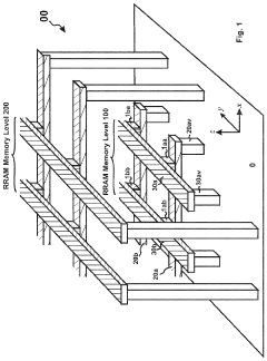
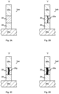
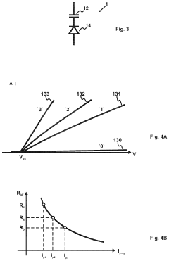
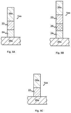
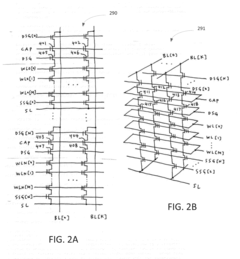
Multi-Bit-Per-Cell Three-Dimensional Resistive Random-Access Memory (3D-RRAM)
PatentActiveUS20200350030A1
Innovation
- The development of a multi-bit-per-cell 3D-RRAM system, where RRAM cells are programmed to have more than two states by adjusting programming currents, and a full-read mode and differential amplifier are implemented to minimize read errors due to leaky cells and external interferences, respectively.
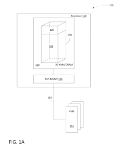
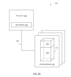
Method and apparatus for providing three-dimensional integrated nonvolatile memory (NVM) and dynamic random access memory (DRAM) memory device
PatentActiveUS20160071591A1
Innovation
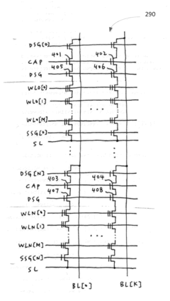
- A hybrid memory system is developed that integrates volatile and nonvolatile memory devices in a stacking configuration, incorporating a drain select gate transistor and a capacitor component, enabling simultaneous data transfer and multi-page programming, and integrating DRAM and NAND cells on a single chip for enhanced performance.
Manufacturing Process Considerations
Manufacturing processes for RRAM and 3D NAND represent fundamentally different approaches to memory fabrication, with significant implications for production costs, scalability, and performance characteristics. RRAM manufacturing leverages relatively simple processes compared to 3D NAND, requiring fewer mask layers and potentially lower capital equipment investments. The fabrication typically involves standard CMOS processes with additional steps for resistive material deposition, which can be integrated into existing semiconductor production lines with moderate modifications.
The simplicity of RRAM's crossbar architecture theoretically enables higher density storage with fewer fabrication steps. However, this advantage is counterbalanced by significant challenges in material uniformity and switching reliability. The resistive switching materials must be deposited with precise thickness control and composition uniformity to ensure consistent performance across billions of memory cells.
In contrast, 3D NAND manufacturing has evolved into an extraordinarily complex process involving hundreds of precise steps. The vertical stacking approach requires sophisticated etching techniques to create high aspect ratio holes through multiple layers, followed by precise deposition of charge trap layers and control gates. As manufacturers push beyond 128 layers toward 200+ layer architectures, these processes become increasingly challenging, requiring advanced lithography and etching capabilities.
The yield management for 3D NAND is particularly demanding due to the multiplicative effect of defects across layers. A single defect in the etching process can potentially affect multiple storage layers, making defect detection and process control critical manufacturing considerations. This complexity translates to higher capital equipment costs but is offset by the mature ecosystem and established high-volume manufacturing infrastructure.
RRAM faces manufacturing challenges related to cycle-to-cycle and device-to-device variability. The stochastic nature of filament formation in resistive materials creates inconsistencies that must be addressed through material engineering and circuit design. Recent advances in atomic layer deposition techniques and novel material systems show promise in improving manufacturing consistency.
From a scaling perspective, 3D NAND has demonstrated remarkable progress through vertical scaling, effectively circumventing the limitations of traditional planar scaling. However, as stacks grow taller, the mechanical stability of these structures becomes increasingly problematic, requiring innovations in stress management and structural support. RRAM potentially offers a more straightforward scaling path through both vertical integration and continued lateral scaling, though material challenges must be overcome to realize this potential.
Energy Efficiency and Sustainability Impact
Energy efficiency has emerged as a critical differentiator between RRAM and 3D NAND technologies, with significant implications for sustainability in the data storage industry. RRAM demonstrates remarkable energy efficiency advantages during read and write operations, consuming approximately 10-100 times less power than comparable 3D NAND solutions. This efficiency stems from RRAM's fundamental operating principle, which requires minimal voltage changes to switch resistance states, contrasting with 3D NAND's energy-intensive charge pumping mechanisms.
The standby power consumption profiles of these technologies reveal further distinctions. RRAM exhibits near-zero leakage current when inactive, whereas 3D NAND requires continuous refresh operations to maintain data integrity, resulting in persistent background power draw even during idle states. This difference becomes increasingly significant in large-scale storage deployments where thousands of memory units operate simultaneously.
Manufacturing sustainability represents another dimension of environmental impact. 3D NAND fabrication involves complex multi-layer deposition processes requiring substantial energy inputs and specialized chemicals. In contrast, RRAM manufacturing typically employs fewer process steps and can potentially integrate with standard CMOS fabrication techniques, reducing overall environmental footprint. Industry analyses suggest RRAM manufacturing may generate 15-30% less carbon emissions per unit storage capacity compared to advanced 3D NAND production.
Device longevity further influences sustainability metrics. While 3D NAND typically endures 1,000-3,000 program/erase cycles before reliability degradation, RRAM technologies have demonstrated endurance capabilities exceeding 10^6 cycles in research prototypes. This extended operational lifespan translates to reduced electronic waste generation and less frequent replacement requirements.
Thermal management considerations also favor RRAM implementations. The lower operating power of RRAM translates directly to reduced heat generation, decreasing cooling requirements in data centers. Thermal modeling studies indicate potential cooling energy savings of 20-40% in RRAM-based storage systems compared to equivalent 3D NAND installations, representing substantial operational cost reductions and environmental benefits.
Looking toward future sustainability improvements, RRAM shows promising compatibility with emerging eco-friendly materials. Research efforts are exploring biodegradable substrates and reduced reliance on rare earth elements, potentially establishing RRAM as the foundation for truly sustainable storage solutions. However, 3D NAND manufacturers continue advancing power optimization techniques, gradually narrowing the efficiency gap through architectural refinements and improved power management algorithms.
Unlock deeper insights with Patsnap Eureka Quick Research — get a full tech report to explore trends and direct your research. Try now!
Generate Your Research Report Instantly with AI Agent
Supercharge your innovation with Patsnap Eureka AI Agent Platform!