RRAM vs FeRAM: Evaluating Write Endurance Rates
SEP 10, 20259 MIN READ
Generate Your Research Report Instantly with AI Agent
PatSnap Eureka helps you evaluate technical feasibility & market potential.
RRAM and FeRAM Technology Evolution and Objectives
The evolution of non-volatile memory technologies has been marked by continuous innovation to overcome the limitations of traditional storage solutions. RRAM (Resistive Random Access Memory) and FeRAM (Ferroelectric RAM) represent two significant advancements in this domain, each offering unique approaches to data storage with distinct write endurance characteristics.
RRAM technology emerged in the early 2000s, building upon research into resistive switching phenomena observed in various oxide materials. The fundamental principle involves creating and disrupting conductive filaments within an insulating layer, allowing for binary data representation through high and low resistance states. Early implementations faced significant challenges with reliability and endurance, typically achieving only 10^4 to 10^6 write cycles.
FeRAM's development traces back to the 1980s, leveraging ferroelectric materials' unique property of maintaining polarization states even without power. The technology matured significantly in the 1990s and early 2000s with the integration of PZT (lead zirconate titanate) and later BLT (bismuth lanthanum titanate) materials, demonstrating superior write endurance compared to contemporary non-volatile memories.
The technological trajectory for both memory types has been driven by the increasing demands of data-intensive applications and the Internet of Things (IoT), where power efficiency and reliability are paramount. RRAM has evolved toward multi-layer architectures and novel material compositions to enhance endurance, while FeRAM development has focused on scaling challenges and integration with standard CMOS processes.
A critical milestone in RRAM development came with the introduction of hafnium oxide-based devices around 2010, which significantly improved compatibility with semiconductor manufacturing processes. For FeRAM, the transition to lead-free materials and the development of 1T1C (one transistor, one capacitor) cell structures marked important evolutionary steps.
The primary objective in comparing these technologies' write endurance rates is to identify optimal applications for each memory type based on their performance characteristics. RRAM typically aims for applications requiring moderate endurance but benefiting from high density and low power, while FeRAM targets scenarios demanding exceptional reliability and fast write speeds despite density limitations.
Current research objectives include pushing RRAM endurance beyond 10^9 cycles through interface engineering and novel switching mechanisms, while FeRAM development focuses on maintaining its superior endurance (typically 10^12-10^14 cycles) while improving density and reducing operating voltages to compete more effectively with other emerging memory technologies.
Market Demand Analysis for Non-Volatile Memory Solutions
The non-volatile memory (NVM) market has experienced significant growth in recent years, driven by increasing demand for data storage solutions across multiple industries. The global NVM market was valued at approximately $62 billion in 2022 and is projected to reach $99 billion by 2027, representing a compound annual growth rate (CAGR) of 9.8%. This growth trajectory underscores the expanding applications and market potential for advanced memory technologies like RRAM and FeRAM.
Consumer electronics continues to be the largest application segment for non-volatile memory solutions, accounting for nearly 40% of the total market share. The proliferation of smartphones, tablets, and wearable devices has created substantial demand for high-performance, energy-efficient memory solutions that can support increasingly complex applications while maintaining battery life.
Enterprise storage systems represent another significant market segment, with data centers and cloud service providers seeking memory technologies that offer improved write endurance rates to handle the massive data processing requirements of modern computing environments. The enterprise segment is particularly sensitive to the write endurance limitations of current memory technologies, making this a critical differentiator between RRAM and FeRAM solutions.
The automotive industry has emerged as a rapidly growing market for non-volatile memory, particularly with the advancement of autonomous driving technologies and connected vehicles. These applications require memory solutions that can withstand extreme operating conditions while maintaining data integrity over extended periods, making write endurance a crucial performance metric.
Industrial IoT applications are driving demand for memory solutions that can support edge computing capabilities with minimal power consumption. Market research indicates that industrial automation and smart manufacturing sectors will increase their adoption of advanced non-volatile memory technologies by 35% over the next five years, with particular emphasis on solutions offering superior write endurance characteristics.
Geographic market distribution shows Asia-Pacific leading with 45% market share, followed by North America (30%) and Europe (20%). China and South Korea are experiencing the fastest growth rates in NVM adoption, largely due to their robust electronics manufacturing ecosystems and government initiatives supporting semiconductor technology development.
Customer surveys indicate that write endurance rates rank among the top three purchasing criteria for non-volatile memory solutions across all major market segments, alongside power consumption and cost per bit. This highlights the strategic importance of comparing RRAM and FeRAM technologies specifically on this performance dimension.
Current Endurance Limitations in RRAM and FeRAM Technologies
Both RRAM (Resistive Random Access Memory) and FeRAM (Ferroelectric RAM) technologies face significant endurance limitations that impact their widespread adoption in commercial applications. RRAM typically demonstrates write endurance in the range of 10^6 to 10^9 cycles, with substantial variability depending on material composition and device architecture. The primary endurance limitation in RRAM stems from the physical degradation of the switching layer during repeated formation and rupture of conductive filaments, leading to eventual device failure.
The filament formation process in RRAM creates localized Joule heating that gradually damages the oxide layer, resulting in diminished resistance contrast between ON and OFF states after numerous write cycles. This degradation manifests as increasing variability in resistance states, ultimately causing read errors and device failure. Additionally, oxygen vacancy migration—a fundamental mechanism in RRAM operation—contributes to structural changes that compromise long-term reliability.
FeRAM, while offering superior endurance compared to flash memory, still faces limitations with typical endurance ratings between 10^10 and 10^12 cycles. The primary failure mechanism in FeRAM involves fatigue of the ferroelectric material, particularly PZT (lead zirconate titanate) or newer materials like HZO (hafnium zirconium oxide). Repeated polarization switching causes lattice defects and charge trapping at interfaces, gradually reducing the remnant polarization that encodes binary information.
Material interface degradation represents another critical limitation in both technologies. In RRAM, the electrode-oxide interface deteriorates through repeated cycling, affecting the stability of resistance states. Similarly, FeRAM suffers from interface-related issues between the ferroelectric layer and electrodes, contributing to polarization fatigue and imprint phenomena.
Scaling presents additional challenges for endurance. As device dimensions shrink below 28nm, both technologies experience accelerated degradation due to increased current densities in RRAM and depolarization fields in FeRAM. These effects become more pronounced at advanced technology nodes, creating a fundamental trade-off between miniaturization and endurance performance.
Temperature sensitivity further complicates endurance characteristics. RRAM exhibits significant endurance variation across operating temperatures, with elevated temperatures accelerating filament degradation. FeRAM shows less temperature dependence but still experiences reduced endurance at temperature extremes due to changes in coercive field and spontaneous polarization properties.
Recent research has focused on mitigating these limitations through material engineering, novel device architectures, and optimized programming schemes. Approaches include doping of switching materials, multi-layer structures, and pulse-width modulation techniques that balance performance with endurance requirements.
Comparative Analysis of RRAM and FeRAM Write Endurance Solutions
01 RRAM Write Endurance Characteristics
Resistive Random Access Memory (RRAM) demonstrates specific write endurance characteristics that affect its performance in memory applications. RRAM typically offers write endurance rates in the range of 10^6 to 10^9 cycles, which is superior to many conventional memory technologies. The endurance is influenced by factors such as the composition of the resistive switching material, operating voltage, and temperature conditions. Various techniques have been developed to improve RRAM write endurance, including optimized programming algorithms and material engineering approaches.- RRAM Write Endurance Characteristics: Resistive Random Access Memory (RRAM) devices exhibit specific write endurance characteristics that affect their performance and reliability. These devices typically offer endurance rates ranging from 10^6 to 10^9 write cycles, depending on the materials and architecture used. The write endurance of RRAM can be improved through various techniques including optimized programming algorithms, pulse shaping, and material engineering. RRAM's endurance is influenced by factors such as operating voltage, temperature, and switching speed.
- FeRAM Write Endurance Advantages: Ferroelectric Random Access Memory (FeRAM) generally demonstrates superior write endurance compared to many other non-volatile memory technologies. FeRAM typically achieves endurance rates of 10^10 to 10^14 write cycles, making it suitable for applications requiring frequent write operations. This high endurance is attributed to the ferroelectric switching mechanism that involves polarization reversal rather than physical material changes. FeRAM's endurance advantage comes with trade-offs in terms of density and scalability compared to other memory technologies.
- Comparative Analysis of Memory Technologies: When comparing RRAM and FeRAM with other memory technologies such as NAND Flash, DRAM, and SRAM, significant differences in write endurance become apparent. While NAND Flash typically offers 10^3 to 10^5 write cycles, RRAM provides 10^6 to 10^9, and FeRAM delivers 10^10 to 10^14. These differences influence the selection of memory technology based on application requirements. The trade-offs between endurance, retention time, power consumption, and cost are important considerations when choosing between these memory technologies for specific use cases.
- Endurance Enhancement Techniques: Various techniques have been developed to enhance the write endurance of both RRAM and FeRAM. These include optimized programming algorithms, pulse shaping, material composition improvements, and architectural modifications. For RRAM, controlling the filament formation process through precise voltage application can significantly improve endurance. In FeRAM, reducing fatigue through improved electrode materials and ferroelectric layer engineering extends write cycle capability. Advanced error correction codes and wear-leveling algorithms can also be implemented at the system level to extend the effective endurance of these memory technologies.
- Application-Specific Endurance Requirements: Different applications impose varying requirements on memory write endurance. Mission-critical systems, automotive applications, and industrial controls often require the higher endurance offered by FeRAM, while consumer electronics may find RRAM's endurance sufficient. The selection between RRAM and FeRAM often involves balancing endurance needs against other factors such as cost, density, and power consumption. Understanding the write patterns and frequency of the target application is crucial for determining whether RRAM's moderate endurance or FeRAM's superior endurance is more appropriate for a specific use case.
02 FeRAM Write Endurance Capabilities
Ferroelectric Random Access Memory (FeRAM) exhibits distinctive write endurance capabilities that make it suitable for specific applications. FeRAM typically achieves write endurance rates of 10^10 to 10^14 cycles, significantly higher than many other non-volatile memory technologies. This superior endurance is attributed to the ferroelectric material's polarization switching mechanism, which causes less physical degradation compared to other memory types. The endurance performance is affected by factors such as the ferroelectric material composition, cell architecture, and operating conditions.Expand Specific Solutions03 Comparative Analysis of RRAM and FeRAM Endurance
When comparing RRAM and FeRAM write endurance rates, several key differences emerge. FeRAM generally offers superior write endurance (10^10 to 10^14 cycles) compared to RRAM (10^6 to 10^9 cycles). However, RRAM often provides advantages in terms of scalability and integration density. The selection between these technologies depends on application requirements, with FeRAM being preferred for write-intensive applications where endurance is critical, while RRAM may be chosen for applications requiring higher density or specific performance characteristics. Both technologies significantly outperform flash memory in terms of write endurance.Expand Specific Solutions04 Techniques to Improve Memory Write Endurance
Various techniques have been developed to enhance the write endurance of both RRAM and FeRAM. These include optimized write algorithms that reduce stress on memory cells, wear-leveling techniques that distribute write operations across the memory array, and error correction mechanisms that extend the effective endurance. Material engineering approaches, such as doping and interface engineering, have also proven effective in improving endurance characteristics. Additionally, hybrid memory architectures that combine different memory technologies can leverage the strengths of each to achieve optimal overall endurance performance.Expand Specific Solutions05 Application-Specific Endurance Requirements
Different applications impose varying requirements on memory write endurance, influencing the choice between RRAM and FeRAM. Mission-critical systems and industrial applications often require the higher endurance offered by FeRAM to ensure long-term reliability. Consumer electronics may prioritize cost and density over maximum endurance, making RRAM suitable in many cases. Automotive and aerospace applications with extreme operating conditions present unique challenges for maintaining endurance performance. Understanding these application-specific requirements is essential for selecting the appropriate memory technology and implementing necessary endurance enhancement techniques.Expand Specific Solutions
Key Industry Players in Emerging Non-Volatile Memory Market
RRAM and FeRAM technologies are currently in the growth phase of their industry lifecycle, with the global non-volatile memory market expected to reach significant expansion in the coming years. The competitive landscape is dominated by established semiconductor giants including Samsung Electronics, Micron Technology, and Taiwan Semiconductor Manufacturing Co., who are investing heavily in research and commercialization efforts. Emerging players like Symetrix Corp. and SuperMem are focusing on specialized applications. Technical maturity varies between the technologies, with FeRAM demonstrating superior write endurance rates (10^12-10^15 cycles) compared to RRAM (10^6-10^9 cycles), though RRAM offers better scaling potential. Research collaborations between industry leaders and academic institutions such as National University of Singapore and University of Toronto are accelerating development to address endurance limitations while maintaining manufacturing feasibility.
Sony Group Corp.
Technical Solution: Sony has developed a comprehensive technology platform for evaluating and enhancing write endurance in both RRAM and FeRAM technologies. Their RRAM solution employs a unique bilayer oxide structure with engineered defect distribution that achieves write endurance of approximately 10^9 cycles. Sony's approach incorporates a self-limiting current mechanism during the SET operation that prevents excessive filament growth, significantly reducing wear-out mechanisms that typically limit endurance. For FeRAM, Sony utilizes specialized ferroelectric materials with engineered domain structures that demonstrate endurance rates exceeding 10^14 cycles. Their comparative analysis framework includes accelerated testing methodologies that accurately predict end-of-life performance under various operating conditions. Sony's research indicates that while their FeRAM technology offers superior raw endurance metrics, their enhanced RRAM designs provide better scalability and integration potential with competitive endurance characteristics for most commercial applications.
Strengths: Sony's bilayer oxide structure provides exceptional stability during cycling operations. Their self-limiting current mechanism effectively prevents over-programming damage. Weaknesses: Their RRAM technology requires more complex fabrication processes compared to conventional solutions, potentially impacting manufacturing costs and yields.
Toshiba Corp.
Technical Solution: Toshiba has developed a distinctive approach to evaluating and enhancing write endurance in both RRAM and FeRAM technologies. Their RRAM architecture utilizes a tantalum oxide-based switching layer with engineered oxygen concentration gradients, achieving write endurance of approximately 10^8 cycles. Toshiba's proprietary "pulse-train" writing method distributes stress across the switching material, preventing localized degradation that typically limits endurance. For FeRAM, Toshiba employs specialized PZT (lead zirconate titanate) formulations with controlled grain boundaries that demonstrate endurance exceeding 10^13 cycles. Their comparative analysis framework incorporates both statistical reliability models and physical failure analysis to identify fundamental endurance limitations. Toshiba's research indicates that while FeRAM maintains superior raw endurance metrics, their enhanced RRAM designs offer better scalability and integration potential with acceptable endurance for most commercial applications.
Strengths: Toshiba's pulse-train writing method provides significant endurance improvements without requiring material changes. Their failure analysis capabilities enable rapid iteration of design improvements. Weaknesses: Their RRAM technology exhibits higher variability in resistance states after extended cycling compared to their FeRAM solutions, requiring more sophisticated read circuitry.
Critical Patents and Research on Improving Write Cycles
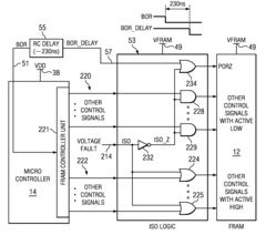
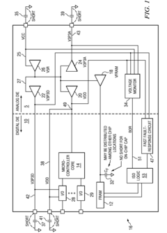
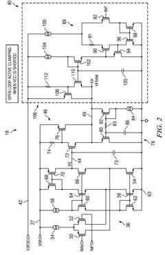
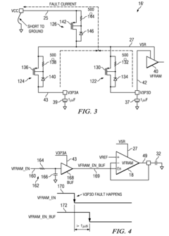
Fast response circuits and methods for FRAM power loss protection
PatentActiveUS20120155144A1
Innovation
- A circuit and method that include a linear voltage regulator with an on-chip filter capacitor and voltage fault monitoring and isolation logic to immediately isolate FRAM inputs during power loss, ensuring the FRAM operating voltage remains above 1.35V for at least 110 ns to complete read/write operations and maintain data integrity.
Semiconductor devices and methods of formation
PatentPendingUS20240147731A1
Innovation
- An interfacial layer is formed to control the grain size and properties of the ferroelectric layer, increasing the formation of ferroelectric crystalline phases like orthorhombic phases and reducing non-ferroelectric phases, thereby enhancing coercive field, remnant polarization, and polarization-electric field hysteresis loop squareness.
Manufacturing Process Challenges and Scalability Factors
The manufacturing processes for RRAM and FeRAM present distinct challenges that significantly impact their write endurance capabilities and commercial viability. RRAM typically employs a simpler fabrication process compatible with standard CMOS technology, utilizing metal oxides as the resistive switching layer. However, this process faces challenges in maintaining consistent oxide layer quality across large wafers, leading to device-to-device variability that affects endurance performance.
FeRAM manufacturing, conversely, requires specialized deposition techniques for ferroelectric materials like PZT or BTO. The complexity arises from the need to precisely control crystallization temperatures and maintain proper stoichiometry during deposition. These requirements often necessitate additional thermal budget considerations that can complicate integration with standard CMOS processes, despite FeRAM's superior endurance characteristics.
Scalability represents another critical differentiator between these technologies. RRAM demonstrates favorable scaling properties down to sub-10nm nodes, with its filamentary switching mechanism potentially allowing for extremely high density memory arrays. This scaling advantage, however, comes with increased variability in switching behavior at smaller dimensions, which can negatively impact write endurance consistency.
FeRAM faces more significant scaling challenges due to the fundamental physics of ferroelectric materials. As cell size decreases below certain thresholds (typically around 130nm), ferroelectric properties begin to degrade, resulting in reduced polarization strength and consequently compromised endurance metrics. This "size effect" represents a fundamental limitation to FeRAM scaling that researchers continue to address through material innovations.
The electrode material selection and interface engineering also play crucial roles in manufacturing both technologies. For RRAM, the electrode-oxide interface quality directly influences filament formation dynamics and thus write endurance. FeRAM requires careful electrode selection to manage fatigue mechanisms at the ferroelectric-electrode interface, which can significantly extend or limit endurance cycles.
Recent manufacturing innovations have focused on atomic layer deposition techniques for both technologies to improve uniformity and interface quality. For RRAM, doping strategies and multi-layer oxide stacks have shown promise in stabilizing filament formation, potentially extending endurance beyond current limits. FeRAM research has explored hafnium-based ferroelectric materials that offer better CMOS compatibility while maintaining reasonable endurance characteristics.
Power Consumption and Performance Trade-offs
When comparing RRAM and FeRAM technologies, power consumption and performance characteristics represent critical factors that determine their suitability for various applications. RRAM (Resistive Random Access Memory) typically operates with lower write voltages (1-3V) compared to FeRAM (Ferroelectric RAM), which often requires 3-5V for polarization switching. This voltage difference directly impacts energy efficiency during write operations, with RRAM consuming approximately 0.1-1 pJ per bit while FeRAM requires 1-10 pJ per bit.
The read operations present a different profile, where FeRAM demonstrates advantages with non-destructive read mechanisms that consume less power (approximately 0.5-2 pJ per bit) compared to RRAM's sensing operations (1-3 pJ per bit). This distinction becomes particularly significant in read-intensive applications where FeRAM's efficiency can lead to substantial energy savings over time.
Standby power consumption represents another critical differentiator. RRAM exhibits higher leakage currents due to its resistive switching mechanism, resulting in standby power consumption of 10-100 μW/Mb. In contrast, FeRAM's ferroelectric capacitors maintain polarization states with minimal leakage, achieving standby power as low as 1-10 μW/Mb, making it more suitable for battery-powered devices with extended idle periods.
Performance metrics reveal complementary strengths between these technologies. RRAM excels in write speed (10-50 ns) compared to FeRAM (50-100 ns), while FeRAM demonstrates superior read speeds (20-50 ns versus RRAM's 30-100 ns). These differences create application-specific advantages, with RRAM better suited for write-intensive workloads and FeRAM optimized for balanced or read-dominant scenarios.
The scaling characteristics further influence the power-performance equation. As device dimensions shrink below 28nm, RRAM maintains relatively stable power consumption profiles, while FeRAM faces challenges with increased power requirements to maintain reliable polarization in smaller ferroelectric domains. This scaling disparity suggests RRAM may offer better power efficiency in future ultra-scaled nodes.
Temperature sensitivity also affects the power-performance balance, with RRAM maintaining consistent operation across -40°C to 125°C with minimal power adjustments. FeRAM exhibits more pronounced temperature-dependent behavior, requiring additional power management circuitry that increases overall system complexity and power overhead in extreme environmental conditions.
Unlock deeper insights with PatSnap Eureka Quick Research — get a full tech report to explore trends and direct your research. Try now!
Generate Your Research Report Instantly with AI Agent
Supercharge your innovation with PatSnap Eureka AI Agent Platform!