

RRAM vs Flash: Which Provides Better Speed & Scalability?
SEP 10, 20259 MIN READ
Generate Your Research Report Instantly with AI Agent
PatSnap Eureka helps you evaluate technical feasibility & market potential.
RRAM and Flash Memory Evolution Background
Memory technology has undergone significant evolution since the introduction of the first electronic storage devices. Flash memory, developed in the 1980s by Toshiba, revolutionized non-volatile storage with its ability to retain data without power. Initially limited in capacity and speed, Flash memory has evolved through multiple generations, from Single-Level Cell (SLC) to Multi-Level Cell (MLC), Triple-Level Cell (TLC), and now Quad-Level Cell (QLC) architectures, each increasing density at the cost of endurance and speed.
The NAND Flash architecture, which dominates today's storage market, has scaled from 130nm to sub-20nm processes, enabling terabyte-scale storage in compact form factors. However, as Flash approaches its physical scaling limits around 10nm, the industry has been exploring alternative memory technologies to overcome these barriers.
Resistive Random-Access Memory (RRAM), also known as ReRAM, emerged as a promising next-generation non-volatile memory technology in the early 2000s. RRAM operates on fundamentally different principles than Flash, utilizing changes in resistance states of a dielectric material rather than storing charge in floating gates. This resistance-based mechanism potentially offers significant advantages in switching speed, power consumption, and scalability.
The evolution of RRAM has been marked by intensive research into various material systems, including metal oxides like HfOx, TaOx, and TiOx. These materials exhibit resistive switching behavior when subjected to appropriate voltage biases, forming conductive filaments that can be repeatedly formed and broken to represent binary data.
While Flash memory has dominated the market for decades, its scaling trajectory faces fundamental physical limitations. As cell sizes shrink below certain dimensions, electron leakage and interference between cells become increasingly problematic, affecting data retention and reliability. Additionally, the program/erase mechanisms in Flash memory involve high voltages that stress the tunnel oxide, limiting endurance to typically 10^3-10^5 cycles for MLC/TLC Flash.
RRAM presents a potential solution to these scaling challenges. Its simple two-terminal structure theoretically allows for denser arrays and three-dimensional stacking. Early research has demonstrated RRAM cells at sub-10nm dimensions, suggesting a path beyond Flash's scaling limits. Furthermore, RRAM's switching mechanism potentially enables faster operation speeds in the nanosecond range, compared to the microsecond-to-millisecond range typical of Flash operations.
The technological evolution of both memory types reflects the semiconductor industry's persistent pursuit of higher density, lower power consumption, and improved performance. As data-intensive applications continue to grow in importance, the limitations of Flash and the potential advantages of emerging technologies like RRAM have become increasingly relevant to the future of computing and storage systems.
Market Demand Analysis for Next-Generation Memory
The global memory market is experiencing a significant shift as traditional storage technologies reach their physical limitations. The demand for next-generation memory solutions is primarily driven by the exponential growth in data generation across various sectors including cloud computing, artificial intelligence, Internet of Things (IoT), and edge computing. Market research indicates that the next-generation memory market is projected to grow at a compound annual growth rate of 29.7% from 2021 to 2026, reaching approximately $13.7 billion by 2026.
Within this landscape, RRAM (Resistive Random Access Memory) and Flash memory represent two competing technologies with distinct market positioning. Flash memory currently dominates the non-volatile memory market with widespread adoption in consumer electronics, data centers, and automotive applications. However, its scaling limitations and performance constraints are creating market opportunities for alternative technologies like RRAM.
The demand for RRAM is particularly strong in applications requiring high-speed operation, low power consumption, and enhanced durability. Industries such as aerospace, defense, and industrial automation are increasingly looking toward RRAM solutions for mission-critical systems where reliability under extreme conditions is paramount. Additionally, the growing artificial intelligence and machine learning sectors require memory solutions capable of handling massive parallel processing tasks, creating a substantial market niche for RRAM technology.
Flash memory continues to maintain strong market demand due to its established ecosystem, manufacturing maturity, and continuous improvements in 3D NAND technology. The consumer electronics segment, particularly smartphones and portable devices, remains heavily reliant on Flash memory solutions due to their cost-effectiveness and adequate performance characteristics for everyday applications.
Regional analysis reveals that Asia-Pacific, particularly Taiwan, South Korea, and China, leads in memory technology manufacturing capacity, while North America dominates in terms of innovation and intellectual property development. European markets show increasing demand for specialized memory solutions in automotive and industrial applications, particularly as electric vehicles and smart manufacturing gain traction.
The enterprise storage segment represents one of the fastest-growing market opportunities for next-generation memory technologies. As organizations increasingly adopt hybrid cloud infrastructures and data-intensive applications, the demand for memory solutions offering improved speed, density, and power efficiency continues to rise. This trend is further accelerated by the proliferation of edge computing architectures, which require distributed memory solutions capable of processing data closer to its source.
Technical Challenges in RRAM and Flash Technologies
Despite significant advancements in both RRAM and Flash memory technologies, several technical challenges continue to impede their optimal performance and widespread adoption. Flash memory, particularly NAND Flash, faces fundamental scaling limitations as cell sizes approach physical boundaries. When cells become too small, electron leakage between adjacent cells increases dramatically, causing data corruption and reliability issues. This phenomenon, known as cell-to-cell interference, becomes more pronounced with each new generation of smaller process nodes.
Flash memory also suffers from endurance limitations, with typical NAND Flash supporting only 3,000-100,000 program/erase cycles before failure. This constraint stems from the physical degradation of the tunnel oxide layer during repeated voltage stress. Additionally, Flash memory's inherent architecture requires block-level erasure before writing new data, resulting in write amplification and performance penalties, particularly in random write scenarios.
For RRAM technology, the primary challenge lies in filament formation variability. The conductive filaments that form and dissolve to store data exhibit inconsistent behavior across cycles and between different cells, leading to reliability concerns. This variability manifests as unstable resistance states, causing potential data retention issues and read errors over time.
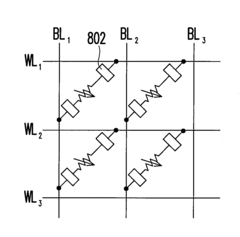
Sneak path currents represent another significant obstacle in RRAM arrays. In crossbar architectures, unintended current paths through adjacent cells can cause misreads and increased power consumption. While selector devices can mitigate this issue, they add complexity and may introduce additional failure modes to the memory system.
Both technologies face material interface challenges. In RRAM, the electrode-oxide interface properties critically influence switching behavior, with degradation at these interfaces leading to performance deterioration over time. Similarly, Flash memory relies on precise interface characteristics between the floating gate and surrounding dielectric materials.
Power consumption during write operations remains problematic for both technologies. Flash memory requires high voltages (15-20V) for programming, while RRAM, though generally more energy-efficient, still demands significant current for reliable filament formation and dissolution. These power requirements limit application in energy-constrained environments such as IoT devices.
Temperature sensitivity affects both technologies differently. RRAM exhibits accelerated filament dissolution at elevated temperatures, potentially causing data loss, while Flash memory experiences faster charge leakage from floating gates as temperature increases. This thermal sensitivity constrains operating environment specifications and necessitates additional error correction mechanisms.
Flash memory also suffers from endurance limitations, with typical NAND Flash supporting only 3,000-100,000 program/erase cycles before failure. This constraint stems from the physical degradation of the tunnel oxide layer during repeated voltage stress. Additionally, Flash memory's inherent architecture requires block-level erasure before writing new data, resulting in write amplification and performance penalties, particularly in random write scenarios.
For RRAM technology, the primary challenge lies in filament formation variability. The conductive filaments that form and dissolve to store data exhibit inconsistent behavior across cycles and between different cells, leading to reliability concerns. This variability manifests as unstable resistance states, causing potential data retention issues and read errors over time.
Sneak path currents represent another significant obstacle in RRAM arrays. In crossbar architectures, unintended current paths through adjacent cells can cause misreads and increased power consumption. While selector devices can mitigate this issue, they add complexity and may introduce additional failure modes to the memory system.
Both technologies face material interface challenges. In RRAM, the electrode-oxide interface properties critically influence switching behavior, with degradation at these interfaces leading to performance deterioration over time. Similarly, Flash memory relies on precise interface characteristics between the floating gate and surrounding dielectric materials.
Power consumption during write operations remains problematic for both technologies. Flash memory requires high voltages (15-20V) for programming, while RRAM, though generally more energy-efficient, still demands significant current for reliable filament formation and dissolution. These power requirements limit application in energy-constrained environments such as IoT devices.
Temperature sensitivity affects both technologies differently. RRAM exhibits accelerated filament dissolution at elevated temperatures, potentially causing data loss, while Flash memory experiences faster charge leakage from floating gates as temperature increases. This thermal sensitivity constrains operating environment specifications and necessitates additional error correction mechanisms.
Current RRAM and Flash Implementation Solutions
01 RRAM speed advantages over Flash memory
Resistive Random Access Memory (RRAM) offers significant speed advantages compared to traditional Flash memory. RRAM devices can achieve faster read and write operations due to their simpler switching mechanism that doesn't require electron tunneling. The resistance-based storage mechanism allows for quicker data access and programming times, with some implementations demonstrating operation speeds in nanoseconds compared to the milliseconds required for Flash operations. This speed improvement makes RRAM particularly suitable for applications requiring rapid data processing and real-time operations.- RRAM speed advantages over Flash memory: Resistive Random Access Memory (RRAM) offers significant speed advantages compared to traditional Flash memory. RRAM devices can achieve faster read and write operations due to their simpler switching mechanism that doesn't require the high voltages needed for Flash memory operations. The resistive switching in RRAM occurs on nanosecond timescales, enabling high-speed data access and programming that can be orders of magnitude faster than Flash memory, making RRAM particularly suitable for applications requiring rapid data processing and real-time operations.
- Scalability improvements in RRAM technology: RRAM technology demonstrates superior scalability compared to Flash memory, allowing for higher density memory arrays. The simple two-terminal structure of RRAM cells enables smaller feature sizes and three-dimensional integration. As device dimensions shrink, RRAM maintains its performance characteristics better than Flash memory, which faces increasing challenges with electron leakage at smaller nodes. This scalability advantage allows RRAM to achieve higher storage densities while maintaining reliability, making it a promising candidate for future memory applications requiring extreme miniaturization.
- Hybrid memory systems combining RRAM and Flash: Hybrid memory architectures that integrate both RRAM and Flash technologies leverage the complementary strengths of each memory type. These systems typically use RRAM for speed-critical operations while utilizing Flash for high-density, non-volatile storage. The combination allows for optimized performance across different workloads, with RRAM handling frequently accessed data and Flash storing less frequently accessed information. Such hybrid approaches can significantly improve overall system performance while managing power consumption and cost considerations effectively.
- Advanced RRAM cell structures for enhanced performance: Innovative RRAM cell structures have been developed to enhance performance metrics including speed and scalability. These designs incorporate novel materials, electrode configurations, and switching layer compositions to optimize resistive switching behavior. Multi-layer structures, engineered interfaces, and doped switching materials can significantly improve switching speed, endurance, and retention characteristics. These advanced cell architectures enable RRAM to achieve performance levels that increasingly outpace traditional Flash memory while maintaining compatibility with standard semiconductor manufacturing processes.
- Memory controller optimizations for RRAM implementation: Specialized memory controllers designed for RRAM implementation address the unique operational characteristics of resistive memory to maximize speed advantages. These controllers incorporate optimized read/write algorithms, voltage management systems, and error correction techniques specifically tailored to RRAM's switching mechanisms. Advanced controllers can dynamically adjust operating parameters based on cell conditions, implement wear-leveling techniques, and manage variability issues inherent to RRAM technology. These controller optimizations are crucial for fully realizing RRAM's theoretical speed and scalability advantages in practical memory systems.
02 Scalability improvements in RRAM technology
RRAM technology offers superior scalability compared to Flash memory, allowing for higher density storage solutions. The simple two-terminal structure of RRAM cells enables smaller feature sizes and three-dimensional integration. Unlike Flash memory that faces scaling limitations due to charge storage mechanisms, RRAM can be scaled down to nanometer dimensions while maintaining performance characteristics. This scalability advantage allows for higher capacity memory arrays in smaller form factors, supporting the continued miniaturization of electronic devices while increasing storage capacity.Expand Specific Solutions03 Hybrid memory systems combining RRAM and Flash
Hybrid memory architectures that integrate both RRAM and Flash technologies leverage the strengths of each memory type. These systems typically use RRAM for speed-critical operations while utilizing Flash for high-density, non-volatile storage. The combination allows for optimized performance in various applications, with RRAM serving as a cache or buffer for frequently accessed data while Flash provides mass storage capabilities. Such hybrid approaches enable improved overall system performance while managing power consumption and maintaining cost-effectiveness in memory subsystems.Expand Specific Solutions04 Advanced RRAM cell structures for enhanced performance
Innovative RRAM cell structures have been developed to enhance performance metrics including speed and scalability. These designs incorporate novel materials, electrode configurations, and switching mechanisms to improve operational characteristics. Multi-layer structures, specialized oxide materials, and engineered interfaces contribute to more reliable switching behavior, reduced variability, and improved endurance. Some advanced designs also address issues like sneak path currents in crossbar arrays and reduce power consumption during switching operations, further enhancing the viability of RRAM for next-generation memory applications.Expand Specific Solutions05 Manufacturing and integration challenges comparison
The manufacturing and integration challenges differ significantly between RRAM and Flash memory technologies. While Flash memory benefits from decades of established manufacturing processes, RRAM presents new integration challenges including material compatibility with CMOS processes, forming voltage requirements, and reliability concerns. However, RRAM offers advantages in terms of back-end-of-line integration potential and fewer mask layers in some implementations. The transition from Flash to RRAM in commercial applications requires addressing these manufacturing challenges while leveraging RRAM's inherent advantages in speed and scalability to justify the technology shift.Expand Specific Solutions
Key Industry Players in Non-Volatile Memory Market
The RRAM vs Flash memory technology landscape is currently in a transitional phase, with RRAM emerging as a promising next-generation non-volatile memory solution. The global market for advanced memory technologies is expanding rapidly, projected to reach significant growth as data-intensive applications proliferate. While Flash memory dominates current storage solutions with mature manufacturing processes led by Samsung, Intel, and Cypress Semiconductor, RRAM offers superior theoretical advantages in speed, power consumption, and scalability. Research institutions like MIT, IMEC, and Chinese research centers are advancing RRAM development, while companies including IBM, Hewlett Packard Enterprise, and Yangtze Memory Technologies are investing heavily in commercialization efforts. The technology is approaching commercial viability, with early applications emerging in specialized markets, though widespread adoption faces challenges in manufacturing consistency and cost-effectiveness compared to established Flash technologies.
Intel Corp.
Technical Solution: Intel has developed 3D XPoint technology (marketed as Optane), which sits between RRAM and Flash in the memory hierarchy. Their solution combines attributes of both technologies, offering non-volatile storage with DRAM-like performance. Intel's approach uses phase change material that switches resistance states when electrical current is applied. Their technology achieves read latencies of approximately 10 microseconds compared to NAND Flash's 100 microseconds, and write latencies of about 20 microseconds versus Flash's millisecond-range performance. Intel has demonstrated endurance ratings of up to 10^7 cycles, significantly outperforming traditional Flash memory's 10^3-10^5 cycle limitation. The company has implemented this technology in both storage and memory products, positioning it as a bridge between storage and memory tiers.
Strengths: Superior performance compared to Flash with 10x lower latency; higher endurance cycles; byte-addressable unlike Flash. Weaknesses: Higher cost per GB than NAND Flash; lower density than current 3D NAND implementations; requires specialized controllers and software optimization to fully leverage performance benefits.
Samsung Electronics Co., Ltd.
Technical Solution: Samsung has invested heavily in both advanced Flash technology and RRAM research. Their current Flash solution focuses on V-NAND (vertical NAND) technology that stacks memory cells vertically in 3D structures, now reaching over 176 layers. This approach achieves densities exceeding 512Gb per die while improving performance and reliability. For RRAM, Samsung has developed cross-point array structures using metal-oxide materials that demonstrate switching speeds below 10ns, compared to Flash's microsecond-range operations. Their RRAM prototypes have shown write endurance exceeding 10^9 cycles and data retention of over 10 years at 85°C. Samsung's research indicates their RRAM technology could potentially achieve 10-100x faster operation than Flash while consuming approximately 1/10th the energy per bit operation. The company has demonstrated working RRAM arrays at 4F² cell sizes, suggesting potential for higher density than current Flash implementations.
Strengths: Established manufacturing infrastructure that can be adapted for RRAM production; comprehensive IP portfolio covering both technologies; financial resources to commercialize emerging memory solutions. Weaknesses: Heavy investment in Flash technology creates potential reluctance to cannibalize existing product lines; RRAM solutions not yet commercially viable at competitive price points.
Critical Patents and Research in Memory Technologies
Resistive memory cell and operation thereof, and resistive memory and operation and fabrication thereof
PatentInactiveUS20120020140A1
Innovation
- The use of conductive domain walls in high-resistance ferroelectric materials, such as BiFeO3, to store data by applying voltage pulses and forming domains with varying polarities, allowing for efficient data storage with reduced power consumption.
Power Efficiency Comparison Between RRAM and Flash
Power efficiency represents a critical factor in memory technology evaluation, particularly when comparing RRAM (Resistive Random Access Memory) and Flash memory technologies. RRAM demonstrates significant power advantages during both read and write operations compared to conventional Flash memory systems. During read operations, RRAM typically consumes 10-100 times less power than NAND Flash, primarily due to its fundamentally different operational mechanism that doesn't require charge pumping or high voltages to detect stored information.
Write operations showcase even more dramatic differences in power consumption. RRAM write operations generally require 100-1000 times less energy than Flash programming operations. This substantial efficiency gap stems from Flash's requirement for high programming voltages (typically 15-20V) and the energy-intensive process of electron tunneling through an insulating layer. In contrast, RRAM's conductive filament formation/dissolution process operates at much lower voltages (typically 1-3V), resulting in significantly reduced power demands.
Standby power consumption also favors RRAM technology. Flash memory requires periodic refresh operations to maintain data integrity, consuming background power even when not actively accessed. RRAM's non-volatile nature eliminates this requirement, allowing for near-zero standby power in idle states, which proves particularly valuable in battery-powered and IoT applications where devices may remain dormant for extended periods.
System-level power efficiency further enhances RRAM's advantages. The faster write speeds of RRAM mean that the memory system remains in active power states for shorter durations, reducing overall energy consumption for equivalent data operations. Additionally, RRAM's ability to perform in-memory computing operations can dramatically reduce data movement between memory and processing units, addressing one of the most power-hungry aspects of modern computing architectures.
Temperature performance also impacts power efficiency considerations. RRAM maintains stable operation across a wider temperature range than Flash, which typically requires additional power for reliable operation at temperature extremes. This characteristic makes RRAM particularly suitable for automotive, industrial, and other harsh environment applications where temperature fluctuations are common.
Looking toward future developments, the scaling advantages of RRAM suggest its power efficiency benefits will likely increase with continued miniaturization, while Flash faces fundamental physical limitations that may require increased power to overcome reliability issues at smaller nodes. This trajectory indicates RRAM's power efficiency advantage may expand further as both technologies continue to evolve.
Manufacturing Process and Cost Analysis
The manufacturing processes for RRAM and Flash memory technologies represent significant differentiating factors in their commercial viability and market adoption. Flash memory manufacturing has benefited from decades of refinement, with established fabrication facilities and mature supply chains. The current 3D NAND Flash manufacturing process involves complex vertical stacking of memory cells, requiring precise etching techniques and specialized equipment. This vertical integration has allowed manufacturers to increase density while maintaining reasonable production costs, achieving economies of scale that result in approximately $0.10 per gigabyte for consumer-grade products.
In contrast, RRAM manufacturing processes are still evolving, with various approaches being explored by different manufacturers. The fundamental RRAM structure consists of a metal-insulator-metal (MIM) stack, which theoretically requires fewer processing steps than Flash memory. This simpler structure potentially translates to lower manufacturing costs once production volumes reach comparable levels. Current estimates suggest that at scale, RRAM could achieve a 30-40% cost reduction compared to equivalent Flash memory solutions.
A key manufacturing advantage for RRAM is its compatibility with standard CMOS back-end-of-line (BEOL) processes. This compatibility enables RRAM to be integrated into existing semiconductor manufacturing facilities with minimal retooling, reducing the capital expenditure required for mass production. Additionally, RRAM can be fabricated at lower temperatures than Flash, potentially reducing energy consumption and associated manufacturing costs.
Yield rates represent another critical manufacturing consideration. Current Flash memory manufacturing achieves impressive yield rates exceeding 90% for mature processes. RRAM manufacturing yields remain lower, typically in the 60-75% range for leading manufacturers, though these figures continue to improve as the technology matures. This yield gap contributes significantly to the current cost differential between the technologies.
Material costs also factor into the manufacturing equation. RRAM utilizes various metal oxides as the switching medium, including HfO₂, TiO₂, and Ta₂O₅. While these materials are not inherently expensive, the precise deposition and quality control requirements add to manufacturing complexity. Flash memory, despite requiring more processing steps, benefits from highly optimized material sourcing and processing techniques developed over decades of production refinement.
Looking forward, the manufacturing cost trajectory favors RRAM as production volumes increase and processes mature. Industry analysts project that RRAM manufacturing costs could undercut Flash memory by 2025-2027, assuming continued investment in manufacturing technology and increasing adoption in specialized applications. This cost advantage, combined with RRAM's performance benefits, positions it as a potentially disruptive technology in the non-volatile memory market, particularly for applications where speed and scalability justify premium pricing during the technology's early adoption phase.
Unlock deeper insights with PatSnap Eureka Quick Research — get a full tech report to explore trends and direct your research. Try now!
Generate Your Research Report Instantly with AI Agent
Supercharge your innovation with PatSnap Eureka AI Agent Platform!