RRAM vs Magnetic RAM: Evaluating Data Capacity
SEP 10, 20259 MIN READ
Generate Your Research Report Instantly with AI Agent
PatSnap Eureka helps you evaluate technical feasibility & market potential.
RRAM and MRAM Technology Evolution and Objectives
Resistive Random Access Memory (RRAM) and Magnetic Random Access Memory (MRAM) represent two significant non-volatile memory technologies that have evolved considerably over the past decades. RRAM, which emerged in the early 2000s, operates on the principle of resistance switching in a dielectric material, typically metal oxides like HfO2, TiO2, or Ta2O5. The technology has progressed from simple binary switching mechanisms to more complex multi-level cell configurations, enabling higher data density.
MRAM's development trajectory began in the 1990s with the discovery of giant magnetoresistance (GMR), followed by tunnel magnetoresistance (TMR) in magnetic tunnel junctions (MTJs). The evolution continued with the introduction of spin-transfer torque (STT) mechanisms in the 2000s, which significantly reduced power consumption and improved scalability. More recently, spin-orbit torque (SOT) MRAM has emerged as a promising variant with enhanced endurance characteristics.
The technological objectives for both memory types have consistently focused on increasing data capacity while maintaining reliability and performance. For RRAM, key objectives include improving retention time, which currently ranges from 10 to 100 years depending on the implementation, and addressing variability issues that affect multi-level cell operations. Additionally, researchers aim to reduce the forming voltage and enhance endurance beyond the current 10^6-10^9 cycles.
MRAM's objectives center on increasing storage density while preserving its inherent advantages of unlimited endurance and fast operation speeds. Current research focuses on reducing the critical switching current density, which directly impacts power consumption and cell size. Another significant goal is improving thermal stability to maintain data integrity at smaller node sizes, particularly as dimensions approach sub-20nm.
The convergence of these technologies with conventional CMOS processes represents another crucial evolutionary aspect. Both RRAM and MRAM have made substantial progress in back-end-of-line (BEOL) integration, allowing them to be fabricated above traditional logic circuits. This 3D integration capability potentially enables higher memory density per unit area, addressing one of the fundamental limitations in scaling conventional memory technologies.
Looking forward, the evolution of these technologies is increasingly driven by emerging applications in edge computing, artificial intelligence, and Internet of Things (IoT) devices, which demand memory solutions with both high capacity and energy efficiency. The trajectory suggests a continued focus on materials engineering and novel device architectures to overcome current limitations in data capacity while maintaining the inherent advantages of non-volatility.
Market Demand Analysis for Next-Generation Memory Solutions
The global memory market is experiencing a significant shift as traditional memory technologies approach their physical limitations. The demand for next-generation memory solutions, particularly RRAM (Resistive Random Access Memory) and MRAM (Magnetic Random Access Memory), is being driven by several converging factors in the technology landscape. These emerging non-volatile memory technologies are positioned to address critical gaps in current memory hierarchies.
Data center operators are increasingly seeking memory solutions with higher density and lower power consumption as they face exponential growth in data processing requirements. The global data center memory market is projected to grow at a compound annual growth rate of 22% through 2026, with non-volatile memory technologies expected to capture an increasing share of this expansion.
Mobile device manufacturers represent another significant market segment driving demand for advanced memory solutions. As smartphones and tablets continue to require greater processing capabilities while maintaining or extending battery life, the appeal of RRAM and MRAM's non-volatility and power efficiency becomes particularly compelling. Industry analysts estimate that mobile applications could account for approximately 30% of next-generation memory adoption by 2025.
The automotive sector presents a rapidly expanding market opportunity, particularly with the rise of autonomous vehicles and advanced driver assistance systems. These applications demand memory solutions capable of withstanding extreme operating conditions while delivering reliable, high-speed data access. The automotive memory market is expected to grow substantially, with particular emphasis on technologies offering radiation hardness and temperature stability—areas where both RRAM and MRAM demonstrate advantages over conventional solutions.
Internet of Things (IoT) deployments represent perhaps the most diverse market opportunity. From industrial sensors to consumer wearables, IoT devices typically operate under strict power constraints while requiring persistent data storage. The combination of low power operation and non-volatility makes next-generation memory technologies particularly well-suited for these applications.
Enterprise storage systems are increasingly implementing tiered memory architectures, creating demand for technologies that can bridge the performance gap between DRAM and NAND flash. Both RRAM and MRAM are being evaluated as potential "storage class memory" solutions that could significantly reduce latency in data-intensive applications.
Artificial intelligence and machine learning workloads present unique memory requirements, with training and inference operations demanding high bandwidth, low latency, and significant data capacity. The market for specialized AI memory solutions is projected to grow substantially as these workloads become increasingly prevalent across industries.
Current State and Technical Challenges in Non-Volatile Memory
Non-volatile memory (NVM) technologies have evolved significantly over the past decade, with RRAM (Resistive Random Access Memory) and MRAM (Magnetic Random Access Memory) emerging as promising alternatives to traditional flash memory. Currently, the global NVM market is dominated by NAND and NOR flash technologies, which face inherent scaling limitations as device dimensions approach physical boundaries. These limitations have accelerated research into alternative NVM solutions that offer better scalability, endurance, and power efficiency.
RRAM technology has demonstrated considerable progress, with devices achieving sub-10nm feature sizes in laboratory settings. Commercial RRAM products typically offer storage densities ranging from 1-8Gb per die, with write endurance of 10^5-10^6 cycles. However, RRAM faces significant challenges including resistance drift over time, variability in switching behavior, and sneak path current issues in crossbar arrays that limit practical array sizes.
MRAM technology, particularly Spin-Transfer Torque MRAM (STT-MRAM), has reached commercial production with densities up to 1Gb. Recent advancements in perpendicular magnetic anisotropy materials have improved thermal stability and reduced switching current requirements. While MRAM offers superior endurance (>10^12 cycles) compared to RRAM, it struggles with scaling below 20nm due to the difficulty in maintaining sufficient energy barriers for long-term data retention at smaller dimensions.
The geographical distribution of NVM technology development shows concentration in East Asia (particularly Japan, South Korea, and Taiwan) for manufacturing infrastructure, while North America leads in fundamental research and IP generation. European research institutions have made significant contributions to materials science aspects of both technologies.
A critical technical challenge for both RRAM and MRAM is the data capacity versus reliability trade-off. As cell sizes decrease to increase capacity, both technologies experience degradation in performance metrics. RRAM suffers from increased variability and reduced signal-to-noise ratio, while MRAM faces superparamagnetic limits and increased thermal instability at smaller dimensions.
Power consumption presents another significant challenge, particularly for mobile and IoT applications. While MRAM offers lower write energy compared to flash memory, its read operations consume more power than RRAM. Conversely, RRAM's write operations require higher voltages that complicate power management circuitry.
Integration with CMOS technology remains a hurdle for widespread adoption. RRAM benefits from simpler fabrication processes but faces yield issues at high densities. MRAM requires specialized deposition equipment and precise control of magnetic materials, increasing manufacturing complexity and cost, though recent advancements in manufacturing processes have improved compatibility with standard semiconductor fabrication lines.
Comparative Analysis of RRAM and MRAM Architectures
01 RRAM storage capacity enhancement techniques
Various techniques can be employed to enhance the storage capacity of Resistive Random Access Memory (RRAM). These include multi-level cell configurations that allow storing multiple bits per memory cell, advanced material engineering for improved resistance states, and innovative cell architectures. These approaches enable higher data density while maintaining reliability and performance characteristics of RRAM devices.- RRAM storage capacity enhancement techniques: Various techniques can be employed to enhance the storage capacity of Resistive Random Access Memory (RRAM). These include multi-level cell architectures that allow storing multiple bits per memory cell, advanced material engineering to improve resistance states, and 3D stacking technologies that increase density without expanding the footprint. These approaches collectively enable RRAM to achieve higher data capacities while maintaining performance characteristics.
- MRAM data capacity optimization methods: Magnetic Random Access Memory (MRAM) data capacity can be optimized through several methods including perpendicular magnetic anisotropy designs, spin-transfer torque mechanisms, and multi-bit storage techniques. These approaches allow for higher bit densities while maintaining the non-volatile characteristics of magnetic storage. Advanced cell structures and materials can further enhance the storage density of MRAM devices.
- Hybrid memory architectures combining RRAM and MRAM: Hybrid memory architectures that combine the advantages of both RRAM and MRAM technologies can achieve superior data capacity and performance. These systems leverage the high-speed operation of MRAM with the high-density capabilities of RRAM. Such hybrid approaches often implement tiered memory structures where frequently accessed data resides in faster memory while less frequently accessed data is stored in higher-capacity memory layers.
- Memory controller designs for high-capacity non-volatile memory: Specialized memory controllers are essential for managing high-capacity RRAM and MRAM systems. These controllers implement advanced algorithms for wear leveling, error correction, and data distribution across memory arrays. They also optimize read/write operations to maximize throughput and minimize power consumption while handling the increased complexity of high-density memory architectures.
- Scaling and manufacturing techniques for high-density memory: Advanced manufacturing processes are critical for achieving high data capacities in both RRAM and MRAM technologies. These include nanoscale lithography techniques, precise material deposition methods, and innovative cell designs that minimize feature sizes. Integration with conventional CMOS processes enables cost-effective production while maintaining reliability and performance at higher densities.
02 MRAM data capacity optimization methods
Magnetic Random Access Memory (MRAM) data capacity can be optimized through several methods including perpendicular magnetic anisotropy structures, spin-transfer torque mechanisms, and multi-bit storage techniques. These approaches allow for increased bit density, reduced cell size, and improved thermal stability, ultimately leading to higher capacity magnetic memory devices with enhanced performance characteristics.Expand Specific Solutions03 Hybrid memory architectures combining RRAM and MRAM
Hybrid memory architectures that combine the advantages of both RRAM and MRAM technologies can achieve superior data capacity and performance. These systems leverage the high density of RRAM with the speed and endurance of MRAM to create memory solutions that overcome the limitations of individual technologies. Such hybrid approaches enable optimized memory hierarchies for various computing applications.Expand Specific Solutions04 3D integration for increased memory density
Three-dimensional integration techniques significantly increase the data capacity of both RRAM and MRAM devices. By stacking memory cells vertically rather than expanding horizontally, these approaches achieve higher bit densities without increasing the chip footprint. Advanced fabrication processes enable multiple layers of memory cells with efficient interconnects, resulting in dramatically increased storage capacity per unit area.Expand Specific Solutions05 Memory management and architecture for capacity optimization
Sophisticated memory management techniques and architectural innovations can optimize the effective data capacity of RRAM and MRAM systems. These include advanced error correction codes, wear-leveling algorithms, and intelligent data compression. Additionally, novel memory hierarchies and controller designs can maximize the utilization of physical memory capacity while improving overall system performance and reliability.Expand Specific Solutions
Key Industry Players in Emerging Memory Technologies
The RRAM vs MRAM competitive landscape is characterized by a market in early growth phase, with increasing adoption across memory applications. The global market is projected to reach significant scale as these technologies address limitations of conventional memory solutions. Technologically, major players demonstrate varying maturity levels: Samsung, Toshiba, and SK Hynix lead in RRAM development with production-ready solutions, while Everspin Technologies has established itself as the MRAM pioneer with commercial products. TSMC, GlobalFoundries, and Qualcomm are advancing MRAM integration into semiconductor processes. Research institutions like ITRI and CNRS continue fundamental research, suggesting ongoing innovation potential before market consolidation occurs.
Samsung Electronics Co., Ltd.
Technical Solution: Samsung has developed advanced solutions in both RRAM and MRAM domains to address growing data capacity needs. Their RRAM technology utilizes a proprietary metal oxide-based resistive switching material that enables multi-level cell (MLC) operation, storing up to 3 bits per cell. Samsung's vertical 3D RRAM architecture achieves densities exceeding 1Tb/cm² through stacking multiple layers of memory cells. For MRAM, Samsung has commercialized 28nm STT-MRAM technology with perpendicular magnetic anisotropy (PMA), offering improved thermal stability and reduced switching current. Their MRAM solution achieves write speeds below 10ns while maintaining data retention for over 10 years at operating temperatures. Samsung has integrated MRAM into their embedded memory solutions, demonstrating capacities of 8Mb with plans to scale to higher densities for future applications in IoT, automotive, and AI edge computing.
Strengths: Samsung possesses comprehensive manufacturing infrastructure allowing rapid commercialization of both technologies. Their MRAM solutions offer superior write endurance and speed compared to flash memory. Weaknesses: Samsung's RRAM technology still faces challenges with resistance drift and variability between cells, while their MRAM solutions currently have lower density than competing NAND flash technologies, limiting applications requiring extremely high storage capacity.
Taiwan Semiconductor Manufacturing Co., Ltd.
Technical Solution: TSMC has developed advanced manufacturing processes for both RRAM and MRAM technologies, focusing on their integration with logic circuits for embedded applications. Their RRAM technology utilizes a hafnium oxide-based resistive switching layer compatible with their standard CMOS process flow. TSMC's RRAM implementation achieves cell sizes below 10F² in their 28nm process node, with demonstrated multi-level cell operation storing 2 bits per cell. Their crosspoint architecture enables high-density arrays with minimal peripheral circuitry overhead. For MRAM, TSMC has developed a perpendicular magnetic tunnel junction (pMTJ) process integrated with their 22nm and 16nm technology nodes. Their MRAM solution achieves write speeds below 10ns with data retention exceeding 10 years at 125°C. TSMC has demonstrated functional 8Mb MRAM arrays with bit error rates below 1ppm, suitable for automotive and industrial applications. Their embedded MRAM (eMRAM) technology offers a replacement for embedded flash in SoC designs, providing higher endurance and faster write speeds while maintaining comparable density.
Strengths: TSMC's position as the leading semiconductor foundry enables rapid commercialization and integration of both memory technologies into diverse applications. Their manufacturing expertise allows for consistent quality and yield optimization. Weaknesses: As a foundry, TSMC depends on IP from partners rather than developing fully proprietary solutions, potentially limiting their differentiation. Their current MRAM densities remain lower than NAND flash, restricting applications requiring extremely high storage capacity.
Core Patents and Technical Innovations in Resistive and Magnetic Memory
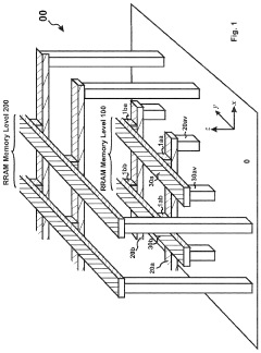
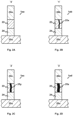
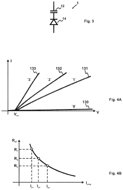
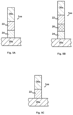
Multi-bit-per-cell three-dimensional resistive random-access memory (3D-RRAM)
PatentActiveUS11170863B2
Innovation
- A multi-bit-per-cell 3D-RRAM design with RRAM cells that can switch between multiple resistance states, using a full-read mode and differential amplifiers to minimize read errors, allowing for more than two states to be stored in each cell and improving reliability under external interferences.
Resistive random-access memory (RRAM) device and forming method thereof
PatentActiveUS11997935B2
Innovation
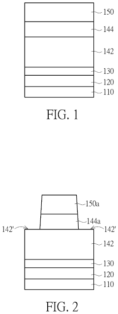
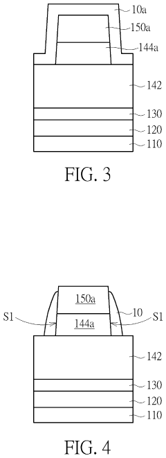
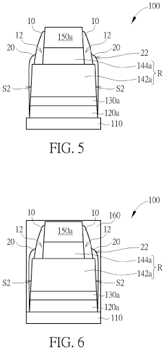
- The formation of two types of spacers, with high work function materials, around the resistive material layers to prevent oxygen diffusion, comprising a method where a bottom electrode, high work function layer, and resistive layers are sequentially deposited and patterned, with spacers covering sidewalls to create a RRAM cell structure.
Manufacturing Scalability and Process Integration Considerations
Manufacturing scalability represents a critical differentiator between RRAM and MRAM technologies when evaluating their potential for high-capacity data storage applications. RRAM offers significant advantages in manufacturing simplicity, as its basic structure consists of a metal-insulator-metal stack that can be fabricated using conventional CMOS processes. This compatibility enables straightforward integration with existing semiconductor manufacturing lines, potentially reducing production costs and accelerating market adoption.
MRAM, while more complex in structure, has demonstrated impressive progress in manufacturing scalability. Major semiconductor foundries including TSMC, Samsung, and GlobalFoundries have successfully integrated MRAM into their production processes, particularly for embedded applications. The magnetic tunnel junction (MTJ) at the core of MRAM requires specialized deposition techniques and precise control of ultra-thin magnetic layers, which initially presented significant yield challenges.
Process integration considerations reveal distinct pathways for each technology. RRAM can be integrated into the back-end-of-line (BEOL) process with relatively few additional steps, making it attractive for 3D stacking applications. This vertical integration capability potentially allows RRAM to achieve higher bit densities per unit area. However, RRAM faces challenges with device-to-device and cycle-to-cycle variability that impact manufacturing yield and reliability.
MRAM integration requires more specialized equipment for depositing and patterning magnetic materials, which increases manufacturing complexity. The thermal budget constraints of MRAM are particularly stringent, as high temperatures during subsequent processing steps can degrade the magnetic properties of the MTJ. This necessitates careful process flow design and potentially limits the flexibility of integration schemes.
Both technologies face scaling challenges as dimensions shrink below 20nm. For RRAM, maintaining reliable switching behavior in smaller cells requires precise control of the conductive filament formation. MRAM encounters challenges with maintaining thermal stability and adequate signal-to-noise ratio as MTJ size decreases. Recent advances in perpendicular magnetic anisotropy materials have improved MRAM's scaling prospects, potentially enabling sub-10nm devices.
The manufacturing ecosystem for both technologies continues to mature, with equipment suppliers developing specialized tools for high-volume production. MRAM currently enjoys stronger industry momentum, with multiple foundries offering embedded MRAM options in their technology nodes. RRAM remains at an earlier stage of manufacturing readiness for high-capacity storage applications, though its simpler structure may ultimately enable more cost-effective scaling for ultra-high density storage.
Energy Efficiency and Performance Metrics Comparison
Energy efficiency represents a critical differentiator between RRAM and MRAM technologies, with significant implications for their deployment in various computing environments. RRAM (Resistive Random Access Memory) demonstrates exceptional energy efficiency during write operations, consuming approximately 0.1-1 pJ per bit, which is substantially lower than conventional flash memory. This efficiency stems from RRAM's fundamental operating principle, where resistance changes occur through the formation and dissolution of conductive filaments without requiring high programming voltages.
In contrast, MRAM (Magnetic RAM) typically requires 2-5 pJ per bit for write operations, making it somewhat less energy-efficient than RRAM in this aspect. However, MRAM compensates with superior read energy metrics, consuming only 0.2-0.5 pJ per bit compared to RRAM's 0.5-1 pJ per bit during read operations. This advantage becomes particularly significant in read-intensive applications where MRAM's overall energy profile may prove more favorable.
Performance metrics beyond energy consumption reveal additional trade-offs between these technologies. RRAM offers write speeds ranging from 10-100 ns, while MRAM achieves faster write operations at 3-20 ns. This speed advantage extends to read operations, where MRAM's 2-20 ns access time outperforms RRAM's 10-50 ns, positioning MRAM as the superior choice for latency-sensitive applications.
Endurance characteristics present another critical performance dimension. MRAM demonstrates exceptional endurance capabilities, supporting 10^12 to 10^15 write cycles before degradation, significantly outperforming RRAM's more limited 10^6 to 10^9 cycle endurance. This substantial difference makes MRAM particularly suitable for write-intensive applications where memory cells undergo frequent state changes.
Temperature stability represents another key performance metric where these technologies diverge. MRAM maintains reliable operation across a wider temperature range (-40°C to 150°C) compared to RRAM's more limited range (-40°C to 85°C), making MRAM the preferred option for automotive, industrial, and aerospace applications where environmental conditions can be extreme.
When evaluating overall system-level efficiency, the integration density and scalability of these technologies must be considered alongside their direct performance metrics. RRAM offers superior scaling potential with demonstrated cell sizes below 10nm, while MRAM faces greater challenges in extreme miniaturization due to the complexity of its magnetic tunnel junction structure. This density advantage potentially allows RRAM-based systems to achieve higher capacity within the same power envelope, offsetting some of its per-bit energy disadvantages.
Unlock deeper insights with PatSnap Eureka Quick Research — get a full tech report to explore trends and direct your research. Try now!
Generate Your Research Report Instantly with AI Agent
Supercharge your innovation with PatSnap Eureka AI Agent Platform!
