

RRAM vs MRAM: Durability and Application Suitability
SEP 10, 20259 MIN READ
Generate Your Research Report Instantly with AI Agent
PatSnap Eureka helps you evaluate technical feasibility & market potential.
Non-Volatile Memory Evolution and Objectives
Non-volatile memory technologies have undergone significant evolution since the introduction of Flash memory in the 1980s. This progression has been driven by increasing demands for higher storage density, faster access speeds, lower power consumption, and greater durability. The memory landscape has expanded beyond traditional Flash to include emerging technologies such as Resistive Random Access Memory (RRAM) and Magnetoresistive Random Access Memory (MRAM), which represent distinct approaches to non-volatile data storage.
RRAM, based on resistance switching phenomena in metal-oxide materials, emerged in the early 2000s as a promising alternative to conventional memory technologies. Its development trajectory has been characterized by incremental improvements in switching reliability, endurance, and retention time. Meanwhile, MRAM, which leverages magnetic tunnel junctions to store data, has evolved from Toggle MRAM to Spin-Transfer Torque MRAM (STT-MRAM) and more recently to Spin-Orbit Torque MRAM (SOT-MRAM), each iteration offering enhanced performance characteristics.
The technological evolution of these memory types reflects broader industry trends toward more efficient computing architectures. As data-intensive applications proliferate across sectors including artificial intelligence, edge computing, and the Internet of Things (IoT), the demand for memory solutions that can balance performance, power efficiency, and reliability has intensified. This evolution is further shaped by the approaching physical limits of traditional scaling methods in semiconductor manufacturing.
Current objectives in non-volatile memory development focus on addressing specific limitations in both RRAM and MRAM technologies. For RRAM, key goals include improving cycling endurance beyond 10^9 cycles, enhancing retention time at elevated temperatures, and reducing variability in resistance states. MRAM development aims to increase storage density while maintaining thermal stability, reducing write energy consumption, and improving scalability to sub-20nm nodes.
Beyond performance metrics, a critical objective is to develop memory solutions tailored to specific application domains. For instance, automotive and industrial applications require exceptional durability under extreme temperature conditions, while IoT devices prioritize ultra-low power consumption. The divergent requirements across these domains necessitate specialized optimization strategies for both RRAM and MRAM technologies.
The ultimate goal of current research efforts is to develop universal memory solutions that combine the best attributes of existing technologies: the speed of SRAM, the density of DRAM, and the non-volatility of Flash, while overcoming the durability limitations that have historically constrained application suitability. This pursuit drives continuous innovation in materials science, device architecture, and manufacturing processes across the memory technology landscape.
Market Analysis for Emerging Memory Technologies
The emerging non-volatile memory (NVM) market is experiencing significant growth, driven by increasing demand for faster, more energy-efficient storage solutions across various industries. Current projections indicate the global NVM market will reach approximately $6.5 billion by 2025, with a compound annual growth rate of nearly 12% from 2020. Within this expanding landscape, RRAM (Resistive Random Access Memory) and MRAM (Magnetoresistive Random Access Memory) represent two of the most promising technologies competing for market share.
RRAM currently holds about 8% of the emerging memory market, with applications primarily in consumer electronics and IoT devices. Its market appeal stems from simple cell structure, low manufacturing costs, and compatibility with conventional CMOS processes. Industry analysts predict RRAM market growth at 15-18% annually through 2025, particularly in edge computing applications where its low power consumption provides competitive advantage.
MRAM, meanwhile, commands approximately 12% of the emerging memory market, with stronger presence in automotive, industrial automation, and enterprise storage sectors. The technology's exceptional endurance characteristics—supporting up to 10^16 write cycles compared to RRAM's 10^6-10^9—position it favorably for applications requiring frequent data updates. MRAM market growth is projected at 22-25% annually through 2025, outpacing RRAM due to its superior reliability metrics.
Regional market distribution shows Asia-Pacific leading RRAM development and adoption, accounting for 45% of global market activity, with particular strength in consumer electronics manufacturing. North America dominates MRAM development with 52% market share, driven by enterprise computing applications and automotive sector growth.
End-user segmentation reveals RRAM gaining traction in consumer wearables, smart home devices, and low-power IoT applications where cost sensitivity outweighs performance requirements. MRAM demonstrates stronger market penetration in mission-critical systems including industrial controllers, automotive safety systems, and enterprise storage arrays where reliability justifies premium pricing.
Market barriers for both technologies include competition from established memory solutions (DRAM, NAND), manufacturing scalability challenges, and integration complexities with existing memory hierarchies. RRAM faces specific market resistance due to endurance limitations, while MRAM adoption is constrained by higher production costs and more complex fabrication requirements.
Industry consolidation is emerging as a significant market trend, with major semiconductor manufacturers acquiring specialized memory startups to secure intellectual property and technical expertise in both RRAM and MRAM development.
RRAM and MRAM Technical Challenges
Both RRAM (Resistive Random Access Memory) and MRAM (Magnetoresistive Random Access Memory) face significant technical challenges that impact their widespread adoption despite their promising characteristics as next-generation non-volatile memory technologies. These challenges span material science, manufacturing processes, and integration complexities.
RRAM encounters substantial durability issues related to its operational mechanism. The formation and rupture of conductive filaments during switching operations gradually degrade the oxide layer, resulting in limited endurance typically ranging from 10^6 to 10^9 cycles. This falls short of requirements for applications demanding high write frequencies. Additionally, RRAM suffers from retention degradation at elevated temperatures, with data potentially becoming unstable above 85°C in many implementations.
The variability in RRAM switching behavior presents another significant challenge. Device-to-device and cycle-to-cycle variations can exceed 20% in resistance states, complicating reliable multi-bit storage and necessitating complex error correction mechanisms that increase system overhead.
MRAM technologies face different but equally challenging issues. The primary limitation for conventional MRAM is the high current density required for switching, which can reach 10^6-10^7 A/cm², creating significant power consumption concerns and limiting scaling potential. While STT-MRAM (Spin-Transfer Torque MRAM) reduces this requirement, it introduces a reliability-speed tradeoff where faster switching increases error rates.
Thermal stability represents a critical challenge for MRAM, particularly as device dimensions shrink below 40nm. Maintaining sufficient energy barriers to prevent spontaneous magnetization reversal while preserving writability becomes increasingly difficult. This fundamental physics constraint limits storage density advancements.
Manufacturing complexities affect both technologies. RRAM requires precise control of defect concentrations in oxide layers, while MRAM demands integration of magnetic materials with standard CMOS processes. The latter introduces contamination risks and requires specialized deposition and etching techniques not standard in conventional semiconductor fabrication.
Application suitability varies significantly between these technologies. RRAM shows promise for neural network implementations due to its analog resistance modulation capability but struggles with the endurance requirements of main memory applications. MRAM offers better endurance and speed characteristics suitable for cache and persistent memory applications but faces challenges in achieving the density and cost metrics necessary to replace NAND flash in storage applications.
Current RRAM and MRAM Implementation Approaches
01 RRAM durability enhancement techniques
Various techniques have been developed to enhance the durability of Resistive Random Access Memory (RRAM). These include optimizing the oxide layer composition, implementing specialized switching mechanisms, and developing new materials for the resistive switching layer. These enhancements help to increase the endurance cycles, improve retention time, and reduce variability in resistance states, ultimately extending the operational lifespan of RRAM devices under repeated write/erase operations.- RRAM durability enhancement techniques: Various techniques can be employed to enhance the durability of Resistive Random Access Memory (RRAM). These include optimizing the oxide layer composition, implementing specialized switching mechanisms, and utilizing novel electrode materials. By controlling the formation and rupture of conductive filaments within the oxide layer, the endurance of RRAM cells can be significantly improved. Additionally, implementing specific programming algorithms and voltage control methods can reduce stress on the memory cells during operation, extending their operational lifetime.
- MRAM durability improvement methods: Magnetic Random Access Memory (MRAM) durability can be improved through several methods focusing on the magnetic tunnel junction (MTJ) structure. These include enhancing the thermal stability of the free layer, optimizing the tunnel barrier thickness, and implementing advanced materials for the reference layer. Techniques such as perpendicular magnetic anisotropy and synthetic antiferromagnetic coupling help maintain data integrity over numerous write cycles. Additionally, specialized write current control mechanisms can reduce wear on the MTJ elements, significantly extending the memory's endurance capabilities.
- Hybrid memory architectures for enhanced durability: Hybrid memory architectures combining RRAM and MRAM technologies can leverage the strengths of both memory types to achieve superior durability. These architectures often employ MRAM for frequently accessed data due to its unlimited endurance and RRAM for less frequently modified data. Intelligent controllers manage data placement and wear leveling across the memory array. Some designs incorporate buffer layers or intermediate caching mechanisms to reduce direct writes to the more vulnerable memory cells, thereby extending the overall system durability while maintaining performance advantages.
- Material innovations for memory durability: Advanced materials play a crucial role in enhancing the durability of both RRAM and MRAM devices. For RRAM, novel oxide materials with controlled defect concentrations and multi-layer structures can improve filament formation stability. In MRAM, specialized magnetic materials with optimized coercivity and thermal stability enhance endurance. Barrier materials that prevent atomic diffusion while maintaining desired electrical properties are also critical. Additionally, interface engineering between different material layers helps reduce degradation mechanisms that occur during repeated cycling, significantly extending the operational lifetime of these memory technologies.
- Circuit design and programming techniques for durability: Specialized circuit designs and programming techniques can significantly enhance the durability of RRAM and MRAM devices. These include adaptive programming algorithms that adjust voltage levels based on cell characteristics, verify-after-write mechanisms to ensure proper state transitions, and error correction codes tailored for these memory types. Advanced sensing circuits can detect early signs of degradation and adjust operating parameters accordingly. Additionally, intelligent refresh schemes and wear-leveling algorithms distribute stress across the memory array, preventing premature failure of frequently accessed cells and extending the overall memory durability.
02 MRAM durability and reliability improvements
Magnetic Random Access Memory (MRAM) durability has been improved through several innovations including enhanced magnetic tunnel junction (MTJ) structures, specialized materials for the free and reference layers, and optimized writing mechanisms. These improvements address issues such as thermal stability, write errors, and read disturbance, resulting in MRAM devices with higher endurance, better data retention, and increased reliability under various operating conditions.Expand Specific Solutions03 Material innovations for memory durability
Novel materials play a crucial role in enhancing the durability of both RRAM and MRAM technologies. Advanced materials such as specialized metal oxides, doped semiconductors, and engineered multilayer structures have been developed to improve switching characteristics, reduce operational voltages, and enhance thermal stability. These material innovations contribute significantly to extending device lifetime, improving cycling endurance, and maintaining consistent performance over time.Expand Specific Solutions04 Structural design improvements for enhanced endurance
Innovative structural designs have been implemented to enhance the endurance of memory cells. These include multi-layer architectures, specialized electrode configurations, and novel cell geometries that distribute stress more evenly during operation. Such structural improvements help to mitigate physical degradation mechanisms like filament rupture in RRAM and layer delamination in MRAM, resulting in devices with significantly improved operational lifetimes and resistance to wear-out failures.Expand Specific Solutions05 Testing and reliability assessment methods
Advanced testing methodologies and reliability assessment techniques have been developed specifically for evaluating RRAM and MRAM durability. These include accelerated aging tests, statistical modeling of failure mechanisms, and specialized characterization techniques to identify degradation patterns. Such methods enable more accurate prediction of device lifetime, better understanding of failure modes, and development of more durable memory technologies through targeted improvements to address specific reliability concerns.Expand Specific Solutions
Leading Companies in Non-Volatile Memory Space
The RRAM vs MRAM competitive landscape is currently in a transitional phase, with the market growing but still relatively niche compared to conventional memory technologies. MRAM technology appears to be gaining momentum with major players like Samsung Electronics, Intel, and TSMC investing significantly in its development, while companies like Avalanche Technology and Crocus Technology are pushing specialized applications. RRAM development is being pursued by companies including Winbond Electronics and Industrial Technology Research Institute. Both technologies are approaching commercial maturity, with MRAM slightly ahead in terms of market readiness, particularly for applications requiring high endurance and non-volatility. The competition is intensifying as these emerging memory technologies aim to address limitations in existing solutions, with specialized players like Shanghai Ciyu and SuperMem focusing on next-generation implementations.
Samsung Electronics Co., Ltd.
Technical Solution: Samsung has developed both RRAM and MRAM technologies with distinct approaches for different application scenarios. For RRAM, Samsung employs a filamentary switching mechanism using metal oxides (primarily HfO2 and Ta2O5) in a crossbar architecture that achieves high density storage. Their RRAM technology demonstrates storage density of 256Gb per die[3], with write endurance of approximately 10^6 cycles. For MRAM, Samsung has commercialized STT-MRAM technology that achieves 8Gb density with endurance exceeding 10^12 cycles[4]. Samsung's perpendicular MTJ design improves thermal stability while reducing power consumption by approximately 30% compared to earlier MRAM implementations. Their embedded MRAM (eMRAM) solution has been integrated at the 28nm node and below, demonstrating compatibility with their foundry processes. Samsung has positioned MRAM for cache memory, IoT devices, and automotive applications where reliability and endurance are critical, while targeting RRAM toward high-density storage applications where cost-per-bit is the primary concern.
Strengths: Comprehensive portfolio covering both technologies, production-ready solutions at advanced nodes, and established manufacturing infrastructure. Samsung can deploy either technology based on specific application requirements. Weaknesses: Their RRAM technology still faces endurance limitations for write-intensive applications, while their MRAM solutions have not yet reached the density levels of competing memory technologies.
Intel Corp.
Technical Solution: Intel has developed 3D XPoint technology (though later sold to Micron) which shares characteristics with RRAM, while also investing significantly in MRAM research. Their MRAM approach focuses on STT-MRAM with perpendicular magnetic anisotropy (PMA) that demonstrates write endurance exceeding 10^11 cycles[5]. Intel's MRAM implementation achieves write latencies of approximately 20ns, positioning it between DRAM and NAND flash in the memory hierarchy. Their technology incorporates advanced materials engineering to improve the tunnel magnetoresistance (TMR) ratio, achieving values above 200%[6], which enhances read reliability and sensing margins. Intel has demonstrated successful integration of MRAM with their 22nm FinFET process technology, showing a path toward embedded non-volatile memory applications. For automotive and industrial applications requiring extended temperature ranges, Intel's MRAM solution maintains data retention at temperatures up to 150°C for 10 years[7], addressing a key durability concern for these markets.
Strengths: Superior thermal stability across wide operating temperature ranges, excellent endurance characteristics, and proven integration with advanced logic processes. Intel's MRAM technology is particularly well-suited for automotive and industrial applications. Weaknesses: Higher manufacturing complexity and cost compared to conventional memory technologies, and lower density than NAND-based storage solutions.
Key Patents and Research in Resistive Memory
Discrete-time analog filtering
PatentWO2016175781A1
Innovation
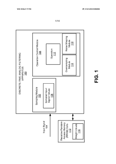
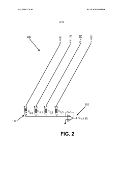
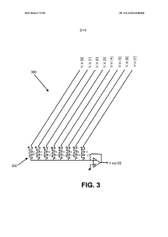
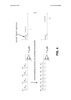
- A discrete-time analog filtering apparatus and method using oversampling and noise shaping to improve accuracy in RRAM cells, where the apparatus includes a sampling module, an operation control module with oversampling and noise shaping capabilities, to efficiently perform Multiply-Accumulate operations and retain accuracy in computations by displacing quantization noise from the baseband into a wider bandwidth.
Semiconductor storage device
PatentWO2016143170A1
Innovation
- The proposed memory system incorporates an ECC circuit and a fuse controller to detect and correct errors in MRAM cells, replacing defective cells with redundancy cells when error correction thresholds are met, ensuring continuous data integrity and system reliability.
Endurance Testing Methodologies
Endurance testing methodologies for RRAM and MRAM technologies require rigorous protocols to accurately assess their durability characteristics under various operational conditions. The fundamental approach involves cycle endurance testing, where memory cells undergo repeated write/erase operations until failure occurs. For RRAM, this typically involves applying voltage pulses to switch between high and low resistance states, while MRAM testing focuses on toggling magnetic orientations through spin-transfer torque or field-induced switching.
Standard endurance testing for both technologies incorporates accelerated life testing, where devices are subjected to elevated temperatures, higher voltages, or increased switching frequencies beyond normal operating conditions. This methodology enables researchers to extrapolate long-term reliability within reasonable testing timeframes. Temperature-dependent testing is particularly critical, as both RRAM and MRAM exhibit different failure mechanisms across temperature ranges.
Data retention testing complements cycle endurance evaluation by assessing how long memory states can be maintained without power. This involves programming devices to known states, storing them at elevated temperatures for extended periods, and subsequently verifying state preservation. For RRAM, retention testing must account for oxygen vacancy migration, while MRAM testing focuses on thermal stability of magnetic configurations.
Statistical analysis forms a crucial component of endurance methodologies, with large sample sizes necessary to account for device-to-device variations. Weibull distribution analysis is commonly employed to characterize failure rates and predict reliability metrics. Advanced testing incorporates in-situ resistance monitoring during cycling to detect gradual degradation patterns before catastrophic failure occurs.
Application-specific testing protocols have emerged to better simulate real-world conditions. For automotive applications, testing includes temperature cycling between -40°C and 150°C, while enterprise storage testing emphasizes sustained high-frequency operations. Mobile device applications require testing under variable power conditions to simulate battery operation.
Recent methodological advances include pulse-train testing, where complex sequences of programming pulses mimic actual application workloads rather than simple alternating patterns. Additionally, combined stress testing applies multiple stressors simultaneously (temperature, voltage, frequency) to identify potential interaction effects that might not appear in single-parameter tests.
Standardization efforts by organizations like JEDEC have established testing frameworks that enable meaningful comparison between different memory technologies and manufacturers, though specialized protocols continue to evolve as these emerging memory technologies mature and target increasingly diverse application spaces.
Industry-Specific Application Requirements
Different industries have distinct requirements for memory technologies, driving the selection between RRAM and MRAM based on specific operational demands. In the automotive sector, memory solutions must withstand extreme temperature ranges (-40°C to 125°C) and maintain data integrity for 10-15 years while enduring constant vibration. MRAM demonstrates superior performance in these harsh conditions due to its inherent temperature stability and virtually unlimited write endurance, making it increasingly preferred for advanced driver-assistance systems and autonomous driving platforms.
The aerospace and defense industries demand radiation-hardened memory with exceptional reliability under cosmic radiation exposure. MRAM's magnetic storage mechanism provides natural radiation resistance compared to RRAM's vulnerability to single-event upsets, positioning MRAM as the preferred solution for satellite systems and military applications where data corruption is unacceptable.
For industrial IoT deployments, power efficiency becomes paramount as devices often operate in remote locations with limited energy sources. RRAM's ultra-low standby power consumption provides advantages for sensors and monitoring equipment that transmit data infrequently but must maintain long-term deployment viability. However, industrial control systems requiring frequent write operations benefit from MRAM's superior endurance characteristics.
The medical device sector presents unique requirements where implantable devices demand both extreme reliability and minimal power consumption. MRAM's non-volatile nature and high endurance make it suitable for critical applications like pacemakers and insulin pumps, where device failure could be life-threatening. Conversely, portable medical diagnostic equipment may leverage RRAM's density advantages for storing larger datasets with less frequent write operations.
Consumer electronics manufacturers prioritize different attributes—balancing cost, density, and performance. RRAM's potential for higher storage density at lower cost positions it favorably for mass-market applications like smartphones and tablets where large storage capacity is valued. Meanwhile, MRAM finds application in premium devices where performance and reliability justify its higher implementation cost.
Data centers and enterprise storage systems increasingly seek non-volatile memory solutions that combine DRAM-like performance with storage persistence. MRAM's faster write speeds and unlimited endurance make it suitable for write-intensive database applications and transaction processing systems, while RRAM may serve effectively in cold storage tiers where density and cost efficiency outweigh performance considerations.
Unlock deeper insights with PatSnap Eureka Quick Research — get a full tech report to explore trends and direct your research. Try now!
Generate Your Research Report Instantly with AI Agent
Supercharge your innovation with PatSnap Eureka AI Agent Platform!