

RRAM vs SRAM: Which Offers Faster Data Access?
SEP 10, 20259 MIN READ
Generate Your Research Report Instantly with AI Agent
PatSnap Eureka helps you evaluate technical feasibility & market potential.
Memory Technology Evolution and Objectives
Memory technology has evolved significantly over the past several decades, transitioning from magnetic core memory in the 1950s to the diverse ecosystem of memory technologies we see today. This evolution has been driven by the increasing demands for faster, more energy-efficient, and higher-density memory solutions to support the exponential growth in computing power and data processing requirements.
The traditional memory hierarchy has long been dominated by SRAM (Static Random-Access Memory) at the cache level and DRAM (Dynamic Random-Access Memory) at the main memory level, with magnetic storage serving as the backbone for long-term data retention. However, this conventional architecture is facing significant challenges as Moore's Law approaches its physical limits and as emerging applications demand ever-increasing memory performance.
SRAM, introduced in the 1960s, has been the gold standard for high-speed cache memory due to its exceptional access speeds, typically in the range of 1-10 nanoseconds. Its six-transistor cell design provides stable data storage without the need for periodic refreshing, making it ideal for performance-critical applications. However, SRAM's relatively large cell size and high leakage power have become increasingly problematic as devices continue to shrink.
In contrast, emerging technologies like RRAM (Resistive Random-Access Memory) represent a new paradigm in memory design. RRAM, which stores data by changing the resistance of a dielectric material, promises to combine the speed advantages of volatile memories with the persistence of non-volatile storage. This technology has garnered significant attention for its potential to bridge the performance gap between memory and storage tiers.
The primary objective of current memory technology research is to overcome the "memory wall" – the growing disparity between processor and memory speeds that has become a critical bottleneck in system performance. Researchers and industry leaders are actively exploring whether RRAM can match or exceed SRAM's access speeds while offering additional benefits such as non-volatility, higher density, and lower power consumption.
Another key goal is the development of universal memory solutions that can potentially replace multiple tiers in the memory hierarchy, simplifying system architecture and reducing costs. RRAM is one of several candidates being evaluated for this role, alongside other emerging technologies such as MRAM (Magnetoresistive RAM), PCM (Phase Change Memory), and FeRAM (Ferroelectric RAM).
As we look toward the future of computing, including neuromorphic systems, quantum computing, and exascale supercomputers, the evolution of memory technology will play a pivotal role in enabling these advanced computing paradigms. The question of whether RRAM can surpass SRAM in access speed is not merely academic but has profound implications for the future architecture of computing systems.
Market Demand Analysis for High-Speed Memory
The high-speed memory market is experiencing unprecedented growth driven by emerging technologies that demand faster data processing capabilities. Current market analysis indicates that the global high-performance memory market is projected to reach $92.4 billion by 2025, growing at a CAGR of approximately 7.3% from 2020. This growth is primarily fueled by the expanding requirements of data centers, artificial intelligence applications, and edge computing devices.
The comparison between RRAM (Resistive Random Access Memory) and SRAM (Static Random Access Memory) represents a critical decision point for manufacturers and system designers seeking optimal performance solutions. Market research shows that while SRAM continues to dominate in applications requiring the absolute fastest access times, RRAM is gaining significant traction due to its promising combination of speed, density, and power efficiency.
Consumer electronics remains the largest market segment for high-speed memory, accounting for approximately 38% of total demand. However, enterprise servers and data centers are showing the fastest growth rate at 9.2% annually, driven by cloud computing expansion and big data analytics requirements. These enterprise applications particularly value the nanosecond-level access times that both RRAM and SRAM can potentially deliver.
Geographic distribution of demand shows North America leading with 34% market share, followed closely by Asia-Pacific at 31%, which is expected to overtake North America by 2026 due to rapid technological adoption in countries like China, South Korea, and Taiwan. The European market accounts for 24% of global demand, with particular emphasis on automotive and industrial applications requiring high-reliability memory solutions.
Industry surveys indicate that 73% of system architects consider access speed as the primary selection criterion for memory technologies in high-performance computing applications. Power efficiency ranks second at 65%, while cost considerations follow at 58%. This prioritization highlights why the RRAM versus SRAM comparison has become increasingly relevant in product development decisions.
The automotive sector represents an emerging high-growth market for high-speed memory, with advanced driver-assistance systems (ADAS) and autonomous driving technologies requiring ultra-fast, reliable memory solutions. Market forecasts suggest automotive memory demand will grow at 12.4% annually through 2025, creating new opportunities for both RRAM and SRAM technologies to demonstrate their respective advantages in access speed and reliability.
RRAM and SRAM Technical Challenges
Despite their widespread adoption, both RRAM (Resistive Random Access Memory) and SRAM (Static Random Access Memory) face significant technical challenges that impact their performance, reliability, and commercial viability. SRAM, as a mature technology, confronts scaling limitations as transistor sizes approach physical boundaries. The 6T SRAM cell architecture requires substantial silicon area, limiting storage density and increasing power consumption as leakage currents become more pronounced at smaller nodes. Additionally, SRAM exhibits vulnerability to soft errors caused by cosmic radiation, particularly problematic in aerospace and mission-critical applications.
SRAM also faces challenges with process variations at advanced nodes, where manufacturing inconsistencies can lead to stability issues, necessitating complex compensation techniques that further increase design complexity and cost. The inherent volatility of SRAM requires constant power to maintain stored data, resulting in significant standby power consumption that becomes increasingly problematic in battery-powered and energy-efficient applications.
RRAM, while promising as an emerging non-volatile memory technology, encounters its own set of formidable challenges. The resistance switching mechanism in RRAM devices often suffers from variability issues, where the same programming conditions can produce different resistance states across devices or even within the same device over time. This variability complicates reliable multi-level cell operation and necessitates sophisticated error correction schemes.
Endurance limitations represent another critical challenge for RRAM, with current technologies typically supporting 10^6 to 10^9 write cycles before failure—significantly lower than SRAM's practically unlimited endurance. This limitation restricts RRAM's applicability in write-intensive applications such as cache memory or high-performance computing systems.
The switching speed of RRAM presents another significant hurdle in competing with SRAM for high-speed applications. While SRAM offers access times in the sub-nanosecond range, RRAM typically operates in the tens to hundreds of nanoseconds, creating a substantial performance gap for time-critical operations. This speed differential becomes particularly problematic when considering RRAM as a direct SRAM replacement in processor caches.
Material stability and integration challenges further complicate RRAM development. Many RRAM designs utilize novel materials that may degrade over time or under extreme conditions, raising reliability concerns. Additionally, integrating these materials into standard CMOS fabrication processes requires overcoming compatibility issues with existing manufacturing equipment and processes, potentially increasing production costs and complexity.
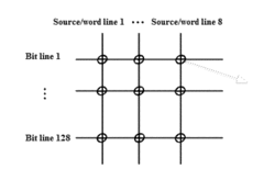
The selector device requirements for RRAM arrays add another layer of complexity. To prevent sneak path currents in crossbar architectures, each RRAM cell typically requires a selector device, which increases cell size and fabrication complexity while potentially limiting the achievable density advantages over conventional memories.
SRAM also faces challenges with process variations at advanced nodes, where manufacturing inconsistencies can lead to stability issues, necessitating complex compensation techniques that further increase design complexity and cost. The inherent volatility of SRAM requires constant power to maintain stored data, resulting in significant standby power consumption that becomes increasingly problematic in battery-powered and energy-efficient applications.
RRAM, while promising as an emerging non-volatile memory technology, encounters its own set of formidable challenges. The resistance switching mechanism in RRAM devices often suffers from variability issues, where the same programming conditions can produce different resistance states across devices or even within the same device over time. This variability complicates reliable multi-level cell operation and necessitates sophisticated error correction schemes.
Endurance limitations represent another critical challenge for RRAM, with current technologies typically supporting 10^6 to 10^9 write cycles before failure—significantly lower than SRAM's practically unlimited endurance. This limitation restricts RRAM's applicability in write-intensive applications such as cache memory or high-performance computing systems.
The switching speed of RRAM presents another significant hurdle in competing with SRAM for high-speed applications. While SRAM offers access times in the sub-nanosecond range, RRAM typically operates in the tens to hundreds of nanoseconds, creating a substantial performance gap for time-critical operations. This speed differential becomes particularly problematic when considering RRAM as a direct SRAM replacement in processor caches.
Material stability and integration challenges further complicate RRAM development. Many RRAM designs utilize novel materials that may degrade over time or under extreme conditions, raising reliability concerns. Additionally, integrating these materials into standard CMOS fabrication processes requires overcoming compatibility issues with existing manufacturing equipment and processes, potentially increasing production costs and complexity.
The selector device requirements for RRAM arrays add another layer of complexity. To prevent sneak path currents in crossbar architectures, each RRAM cell typically requires a selector device, which increases cell size and fabrication complexity while potentially limiting the achievable density advantages over conventional memories.
Current RRAM vs SRAM Solutions
01 RRAM access speed characteristics
Resistive Random Access Memory (RRAM) offers specific access speed characteristics that make it suitable for certain applications. RRAM typically provides faster write speeds compared to some non-volatile memory technologies, though generally slower than SRAM. Its access speed is influenced by the resistance switching mechanism, which involves the formation and rupture of conductive filaments. RRAM's speed-power tradeoff makes it an attractive option for applications where non-volatility and reasonable access speeds are required.- RRAM vs SRAM access speed comparison: Resistive Random Access Memory (RRAM) and Static Random Access Memory (SRAM) have different access speed characteristics. SRAM typically offers faster access speeds compared to RRAM, making it suitable for cache memory and high-performance computing applications. However, RRAM provides advantages in terms of non-volatility and density. The speed difference is primarily due to the different operating mechanisms: SRAM uses transistor-based storage cells while RRAM relies on resistance changes in a dielectric material.
- RRAM architecture optimizations for improved speed: Various architectural optimizations can be implemented to improve RRAM access speeds. These include crossbar array structures, optimized sensing circuits, and advanced selector devices that reduce sneak path currents. Multi-level cell configurations and parallel access techniques can also enhance the effective data access speed of RRAM devices. These optimizations aim to narrow the performance gap between RRAM and faster memory technologies like SRAM.
- Hybrid memory systems combining RRAM and SRAM: Hybrid memory architectures that combine RRAM and SRAM leverage the advantages of both technologies. SRAM can be used for frequently accessed data requiring high-speed operations, while RRAM can store larger datasets that benefit from non-volatility. These hybrid systems often employ intelligent data migration algorithms that move data between the memory types based on access patterns, providing an optimal balance between speed, power consumption, and storage capacity.
- Circuit design techniques for memory access acceleration: Specialized circuit designs can significantly improve data access speeds in both RRAM and SRAM. For SRAM, techniques include sense amplifier optimizations, wordline boosting, and dual-port architectures. For RRAM, advanced read/write circuits, current-mode sensing, and voltage-controlled access methods can enhance performance. Additionally, pipelining techniques and parallel access structures help overcome inherent speed limitations in both memory types.
- Emerging technologies to enhance memory access speed: Novel technologies are being developed to further improve memory access speeds beyond conventional approaches. These include three-dimensional integration of memory cells, advanced materials for RRAM switching layers with faster ion mobility, and new selector devices with improved switching characteristics. Additionally, neuromorphic computing architectures that leverage the analog nature of RRAM can provide alternative computational models with different speed-performance tradeoffs compared to traditional digital memory access patterns.
02 SRAM access speed advantages
Static Random Access Memory (SRAM) is known for its superior access speed compared to most memory technologies. SRAM provides fast read and write operations due to its flip-flop based cell structure that doesn't require refresh cycles. The direct access to stored data without the need for capacitor charging/discharging contributes to its high-speed performance. These characteristics make SRAM particularly valuable for cache memory and applications requiring rapid data access, though at the cost of higher power consumption and larger cell size.Expand Specific Solutions03 Hybrid memory architectures combining RRAM and SRAM
Hybrid memory architectures that combine RRAM and SRAM leverage the advantages of both technologies. SRAM can be used for frequently accessed data requiring high-speed operations, while RRAM can store less frequently accessed data that needs to be retained when power is off. This combination optimizes overall system performance by balancing speed, power consumption, and data retention requirements. Such hybrid approaches are particularly beneficial in applications like edge computing and IoT devices where both speed and non-volatility are important.Expand Specific Solutions04 Access speed enhancement techniques for RRAM
Various techniques have been developed to enhance the access speed of RRAM. These include optimizing the material composition of the resistive switching layer, improving the electrode design, and developing advanced programming algorithms. Circuit-level innovations such as sense amplifier designs specifically tailored for RRAM characteristics can also significantly improve read speeds. Additionally, architectural approaches like parallel access schemes and pipelining techniques can be employed to increase the effective throughput of RRAM-based memory systems.Expand Specific Solutions05 Comparative performance analysis between RRAM and SRAM
Comparative analysis between RRAM and SRAM reveals distinct performance characteristics. While SRAM offers superior access speeds (typically in the range of a few nanoseconds), RRAM provides non-volatility and higher density. RRAM's access speeds, though slower than SRAM, are typically faster than other non-volatile memories like Flash. Power consumption patterns also differ significantly, with SRAM consuming more power during operation but RRAM requiring higher voltage pulses for switching states. These differences make each technology suitable for different tiers in the memory hierarchy based on application requirements.Expand Specific Solutions
Key Memory Semiconductor Players
The RRAM vs SRAM technology landscape is currently in a transitional phase, with SRAM remaining the dominant technology for high-speed data access applications despite RRAM's emerging potential. The global memory market, valued at approximately $120 billion, shows SRAM maintaining leadership in performance-critical applications where access speed is paramount. While SRAM technology is mature and widely implemented by established players like Samsung, Intel, and IBM, RRAM represents a disruptive technology being actively developed by companies including Western Digital, SK hynix, and Taiwan Semiconductor Manufacturing Co. RRAM offers promising advantages in non-volatility and density, but still faces challenges in endurance and manufacturing consistency that limit its competitive position against SRAM's sub-nanosecond access times in high-performance computing applications.
International Business Machines Corp.
Technical Solution: IBM has developed sophisticated RRAM technology through their research division, focusing on creating high-performance non-volatile memory solutions. Their RRAM implementation utilizes phase-change materials and resistive switching mechanisms to store data as different resistance states within memory cells. IBM's RRAM architecture achieves read latencies of approximately 30-50 nanoseconds, which is slower than SRAM but offers significant advantages in density and power consumption[9]. The company has pioneered multi-level cell RRAM technology that can store multiple bits per cell, dramatically increasing storage density compared to conventional binary storage approaches. IBM's RRAM research has demonstrated devices with excellent endurance characteristics, achieving over 10^9 write cycles in laboratory settings, which approaches the durability needed for cache-level applications. Their RRAM technology incorporates advanced materials science innovations, including the use of tantalum oxide-based switching layers that provide improved reliability and performance consistency across a wide temperature range[10].
Strengths: IBM's RRAM technology offers excellent scalability to advanced process nodes, non-volatility that eliminates standby power consumption, and significantly higher density than SRAM (approximately 4-10x depending on implementation). Weaknesses: Despite research advances, IBM's RRAM still exhibits slower write speeds than SRAM (typically 50-200ns vs. 1-3ns for SRAM writes) and faces challenges with variability in resistance states that can affect reliability and require more complex error correction mechanisms.
Intel Corp.
Technical Solution: Intel has developed innovative RRAM (Resistive Random Access Memory) technology that utilizes conductive metal oxide-based memory cells to store data as resistance states. Their 3D XPoint technology, developed in collaboration with Micron, represents a significant advancement in non-volatile memory architecture, positioned between NAND flash and DRAM in the memory hierarchy. Intel's RRAM implementation achieves data access speeds approximately 1,000 times faster than NAND flash while offering 10 times higher density than conventional DRAM[1]. The company has integrated this technology into their Optane product line, which delivers persistent memory with DRAM-like performance characteristics. Intel's RRAM architecture employs a crosspoint structure where memory cells are positioned at the intersection of word lines and bit lines, eliminating the need for transistors at each cell and enabling higher density storage compared to traditional SRAM implementations[2].
Strengths: Intel's RRAM technology offers significantly higher density than SRAM while providing non-volatility and lower power consumption. The technology bridges the performance gap between memory and storage. Weaknesses: Despite improvements, Intel's RRAM still cannot match SRAM's raw access speed (tens of nanoseconds vs. single-digit nanoseconds for SRAM), and has faced manufacturing challenges that have limited widespread adoption.
Core Memory Access Speed Innovations
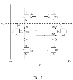
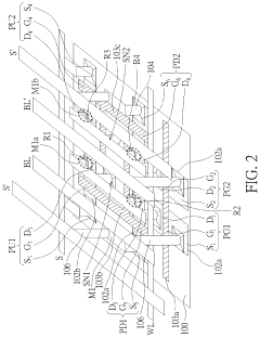
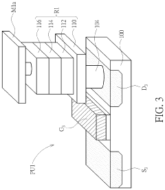
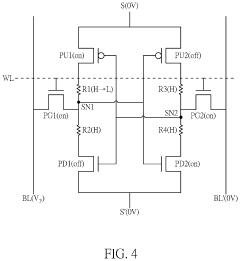
Non-volatile static random access memory incorporating resistive random-access memory
PatentActiveUS11984158B2
Innovation
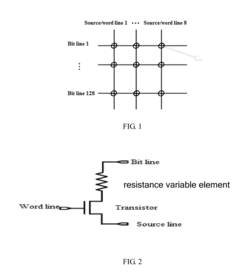
- Incorporating resistive random-access memories (RRAMs) between SRAM storage nodes and transistors, specifically between the drains of pull-up and pull-down transistors, to enable non-volatile storage without increasing the layout area, utilizing a 6T4C architecture with RRAMs positioned for setting contacts and overlapping with transistor drains.
Operation Method of Resistive Random Access Memory and Resistive Random Access Memory Device
PatentActiveUS20180330788A1
Innovation
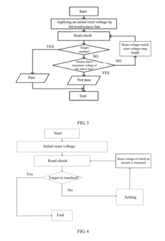
- An operation method for RRAM that involves applying an initial reset voltage, performing a read check to determine if the resistance value reaches a preset target resistance value, and iteratively adjusting the voltage to maintain the storage unit in a low resistance state before resetting, ensuring the resistance value reaches the target high resistance state, thereby preventing rapid relaxation.
Power Efficiency Comparison
Power consumption represents a critical factor in memory technology evaluation, especially in today's energy-conscious computing landscape. SRAM and RRAM exhibit fundamentally different power efficiency profiles due to their distinct operational mechanisms.
SRAM consumes significant dynamic power during active operations, primarily due to its constant need for power to maintain stored data. This continuous power requirement stems from SRAM's volatile nature, where each bit requires multiple transistors (typically six in a 6T configuration) that must remain powered to preserve information. During read and write operations, SRAM cells experience substantial switching activity, further increasing dynamic power consumption.
In contrast, RRAM demonstrates superior power efficiency characteristics in several key aspects. As a non-volatile memory technology, RRAM retains data without power, eliminating the standby power consumption that plagues SRAM implementations. This characteristic makes RRAM particularly advantageous for battery-powered devices and applications with intermittent operation patterns.
Quantitative comparisons reveal RRAM's power advantage, with studies showing power consumption reductions of 10-100x compared to SRAM in certain configurations. For instance, a 28nm RRAM implementation demonstrated power consumption of approximately 0.2pJ per bit operation, while comparable SRAM designs required 2-5pJ per bit operation.
The power efficiency gap becomes even more pronounced in standby scenarios. While SRAM leakage power can account for 30-50% of total system power in modern SoCs, RRAM's zero standby power offers a compelling alternative for power-constrained applications.
However, RRAM's power profile is not without challenges. Write operations in RRAM typically consume more power than read operations due to the physical mechanisms involved in changing resistance states. The SET and RESET operations that modify the conductive filament require relatively high current pulses, though these remain competitive with SRAM's overall power envelope.
Temperature sensitivity also affects power efficiency comparisons. SRAM's leakage power increases exponentially with temperature, while RRAM demonstrates more stable power characteristics across operating temperature ranges, further enhancing its efficiency advantage in high-temperature environments.
For system designers, these power efficiency differences translate directly to battery life extension, thermal management simplification, and potential elimination of cooling infrastructure in certain applications.
Integration Capabilities in Modern Computing Systems
Integration of RRAM and SRAM technologies into modern computing architectures presents distinct challenges and opportunities that significantly impact system performance. SRAM has traditionally dominated cache memory implementations due to its seamless integration with CMOS processes. Modern processors typically incorporate multiple levels of SRAM cache directly on-die, enabling single-cycle access times that are critical for high-performance computing applications.
RRAM integration capabilities, while promising, face several technical hurdles. Current RRAM technologies often require specialized fabrication steps that may not be fully compatible with standard CMOS processes. This has limited their widespread adoption in mainstream computing systems despite their density advantages. However, recent advancements in 3D integration techniques have created new possibilities for RRAM implementation in computing architectures.
The vertical stacking capabilities of RRAM present a significant advantage for system-level integration. Unlike SRAM, which typically requires substantial silicon area in a planar configuration, RRAM can be stacked in multiple layers, potentially offering higher memory density per unit volume. This characteristic makes RRAM particularly attractive for memory-intensive applications where physical space constraints are critical considerations.
Power distribution networks represent another important aspect of integration. SRAM cells require continuous power to maintain stored data, necessitating robust power delivery systems throughout the chip. RRAM's non-volatile nature reduces these requirements, potentially simplifying power distribution architectures and enabling more flexible system designs, particularly for edge computing and IoT applications.
Signal integrity considerations also differ significantly between these technologies. SRAM's well-established integration with CMOS logic allows for optimized signal paths with minimal latency. RRAM interfaces often require additional circuitry for sensing and driving operations, which can introduce signal integrity challenges that must be addressed through careful system design and potentially specialized interface circuits.
Thermal management represents another critical integration factor. SRAM's dynamic power consumption generates heat during active operation, while RRAM's resistive switching mechanisms may produce localized heating effects that require consideration in dense memory arrays. Effective thermal management strategies must be implemented to ensure reliable operation, particularly as integration densities increase.
Looking forward, heterogeneous integration approaches combining both RRAM and SRAM in complementary roles may offer the most promising path for next-generation computing architectures. Such hybrid memory systems could leverage SRAM's speed advantages for performance-critical operations while utilizing RRAM's density and non-volatility for bulk storage functions, creating more efficient and capable computing platforms.
Unlock deeper insights with PatSnap Eureka Quick Research — get a full tech report to explore trends and direct your research. Try now!
Generate Your Research Report Instantly with AI Agent
Supercharge your innovation with PatSnap Eureka AI Agent Platform!