TMDs as Quantum Emitters: Single-Photon Sources for Quantum Communication
AUG 27, 20259 MIN READ
Generate Your Research Report Instantly with AI Agent
Patsnap Eureka helps you evaluate technical feasibility & market potential.
TMDs Quantum Emitter Background and Objectives
Transition metal dichalcogenides (TMDs) have emerged as a revolutionary class of two-dimensional materials that exhibit exceptional optical and electronic properties. Since their initial isolation in 2004, following the groundbreaking work on graphene, TMDs have attracted significant attention due to their direct bandgap in monolayer form, strong light-matter interactions, and unique valley-dependent physics. The evolution of TMD research has progressed from basic material characterization to advanced quantum applications, with quantum emission capabilities being recognized around 2015.
The quantum emission properties of TMDs represent a significant technological advancement in the field of quantum information science. These atomically thin semiconductors, including MoS2, WS2, MoSe2, and WSe2, naturally host defects and strain-induced potential wells that can act as quantum emitters, capable of generating single photons on demand. This capability positions TMDs as promising candidates for next-generation quantum communication systems that require reliable single-photon sources.
The technical trajectory of TMDs as quantum emitters has been marked by several key developments, including the discovery of localized excitons in monolayer WSe2, demonstration of antibunching behavior confirming single-photon emission, and recent advancements in deterministic positioning of quantum emitters through strain engineering and defect creation techniques. These developments have established a foundation for practical quantum applications.
The primary technical objectives in this field include enhancing the quantum emission efficiency, achieving precise control over emitter positioning, improving spectral stability, and developing methods for integrating TMD-based quantum emitters with photonic circuits and existing telecommunication infrastructure. Additionally, there is a strong focus on operating these quantum emitters at higher temperatures, ideally reaching room temperature operation to facilitate practical deployment.
Looking forward, the field aims to develop TMD-based quantum repeaters and quantum networks that can enable long-distance quantum communication by overcoming the current limitations of photon loss in optical fibers. The ultimate goal is to establish quantum communication systems that leverage the unique advantages of TMDs, including their compatibility with silicon photonics, potential for on-chip integration, and the possibility of wafer-scale production.
The convergence of 2D materials science with quantum information technology represents a promising frontier for addressing the challenges of secure communication in the quantum era. As quantum computing advances threaten conventional encryption methods, TMD-based quantum communication offers a pathway to quantum-secure data transmission through fundamentally secure protocols like quantum key distribution.
Quantum Communication Market Analysis
The quantum communication market is experiencing significant growth driven by increasing concerns over data security and the limitations of classical encryption methods. Current market valuations place the global quantum communication sector at approximately 500 million USD in 2023, with projections indicating expansion to reach 3 billion USD by 2030, representing a compound annual growth rate (CAGR) of over 25%.
Government investments constitute a substantial portion of market funding, with the United States, China, and the European Union allocating billions toward quantum communication research and infrastructure development. China has notably invested over 10 billion USD in its quantum initiatives, including the world's first quantum satellite, Micius, demonstrating the strategic importance nations place on this technology.
The commercial sector is increasingly recognizing quantum communication's potential, particularly in banking, defense, healthcare, and telecommunications. Financial institutions are exploring quantum key distribution (QKD) systems to secure transactions, while defense agencies are implementing quantum networks for secure communications. This diversification of application domains is expanding the potential market reach.
Single-photon sources, particularly those based on TMDs (Transition Metal Dichalcogenides), represent a critical component within this market. The demand for reliable, room-temperature quantum emitters is projected to grow at 30% annually, outpacing the overall quantum communication market. TMD-based emitters offer significant advantages in terms of integration potential with existing semiconductor technologies and operational stability.
Market analysis reveals regional variations in adoption patterns. Asia-Pacific leads in implementation, with China at the forefront, followed by North America and Europe. Developing economies are beginning to establish quantum communication research programs, indicating future market expansion beyond current hubs.
Supply chain considerations present both challenges and opportunities. The specialized materials required for TMD-based quantum emitters, including high-purity transition metals and chalcogens, represent a niche but growing market segment valued at approximately 75 million USD annually. Manufacturing scalability remains a key constraint, with current production capabilities limited to research-scale quantities.
Industry experts anticipate a market inflection point between 2025-2027 when quantum communication technologies, including TMD-based single-photon sources, are expected to achieve sufficient reliability and cost-effectiveness for broader commercial deployment. This transition from primarily research applications to commercial implementation will likely trigger accelerated market growth and attract increased private investment.
TMDs Single-Photon Source Technical Challenges
The development of TMDs (Transition Metal Dichalcogenides) as single-photon sources faces several significant technical challenges that currently limit their widespread application in quantum communication systems. These challenges span from material synthesis to operational stability and integration capabilities.
Material quality and consistency remain primary obstacles. The synthesis of atomically thin TMD monolayers with minimal defects requires precise control over growth conditions. Current chemical vapor deposition (CVD) and mechanical exfoliation techniques often produce samples with varying quality, leading to inconsistent quantum emission properties. The presence of unintentional defects, edge irregularities, and substrate interactions can significantly alter the photophysical properties of quantum emitters.
Spectral stability presents another critical challenge. TMD-based single-photon emitters frequently exhibit spectral wandering and blinking behaviors, which compromise their reliability for quantum information applications. This instability stems from charge fluctuations in the surrounding environment and interactions with substrate phonons. While cryogenic operation can mitigate some of these effects, achieving stable room-temperature operation remains elusive.
Deterministic positioning of quantum emitters within TMD materials constitutes a significant engineering hurdle. Current methods rely largely on random defect formation or strain engineering, resulting in unpredictable spatial distribution of emission sites. This randomness complicates the integration of TMD emitters into scalable photonic circuits and devices.
Extraction efficiency limitations further constrain practical applications. The high refractive index contrast between TMDs and their surrounding media leads to poor photon extraction, with much of the emitted light trapped within the material or substrate. While various nanophotonic structures have been proposed to enhance extraction, implementing these solutions while maintaining emitter quality presents considerable fabrication challenges.
Wavelength tunability represents another technical barrier. Most TMD emitters operate in fixed spectral windows determined by their bandgap properties. The ability to precisely tune emission wavelengths to match optimal telecommunication bands or other quantum system requirements remains limited, restricting their versatility in quantum network applications.
Integration with existing photonic and electronic platforms poses additional challenges. Creating hybrid systems that effectively combine TMD emitters with waveguides, detectors, and processing elements requires addressing material compatibility issues, thermal management concerns, and electrical contact formation without degrading emitter performance.
Scalable manufacturing techniques for TMD-based quantum devices are still in their infancy. The transition from laboratory demonstrations to commercially viable production methods necessitates significant advancements in material growth, transfer processes, and device fabrication technologies that maintain quantum emission properties while enabling cost-effective mass production.
Current TMDs Single-Photon Generation Solutions
01 TMD-based quantum emitters for single-photon emission
Transition Metal Dichalcogenides (TMDs) can be engineered to create quantum emitters that produce single photons. These 2D materials, when properly structured with defects or strain, can emit individual photons with high purity and efficiency. The quantum confinement properties of TMDs make them excellent candidates for next-generation quantum light sources, with applications in quantum computing and secure communications.- TMD-based quantum emitters for single-photon emission: Transition Metal Dichalcogenides (TMDs) can be engineered to create quantum emitters that produce single photons. These 2D materials exhibit unique optical properties when defects or strain are introduced, creating localized emission centers. The atomically thin nature of TMDs allows for precise control over quantum confinement effects, resulting in efficient single-photon sources with high purity and indistinguishability, which are essential for quantum information processing applications.
- Strain engineering in TMDs for controlled single-photon emission: Applying mechanical strain to TMD monolayers creates localized exciton trapping sites that can function as single-photon emitters. By precisely controlling the strain profile through nanopatterned substrates or nanostructures, researchers can deterministically position quantum emitters within the TMD material. This approach enables the creation of arrays of single-photon sources with tunable emission properties, which is crucial for integrated quantum photonic circuits.
- Integration of TMD single-photon emitters with photonic structures: TMD-based single-photon emitters can be integrated with photonic structures such as waveguides, cavities, and resonators to enhance emission properties. This integration improves the collection efficiency, directionality, and emission rate of single photons through Purcell enhancement. Coupling TMD quantum emitters with photonic crystals or plasmonic nanostructures enables the development of on-chip quantum light sources with improved performance for quantum communication networks.
- Characterization and measurement techniques for TMD single-photon sources: Advanced characterization techniques are essential for evaluating the performance of TMD-based single-photon emitters. These include Hanbury Brown-Twiss interferometry for measuring photon statistics, time-resolved photoluminescence for determining emission lifetimes, and spectroscopic methods for analyzing emission wavelengths and linewidths. Specialized optical setups and detection systems enable the verification of single-photon emission and assessment of key metrics such as g(2)(0) values, which indicate the quality of the single-photon source.
- Heterostructures and material combinations for enhanced TMD single-photon emission: Creating heterostructures by combining TMDs with other 2D materials or substrates can enhance single-photon emission properties. These engineered structures modify the electronic and optical properties of TMDs through effects such as band alignment, charge transfer, and dielectric screening. Incorporating hexagonal boron nitride as an encapsulation layer or combining different TMD materials in vertical stacks enables the development of single-photon emitters with improved stability, brightness, and spectral purity for quantum technology applications.
02 Fabrication methods for TMD single-photon emitters
Various fabrication techniques can be employed to create single-photon emitters in TMD materials. These include creating localized strain using nanopillars, introducing defects through ion bombardment, and developing heterostructures with other 2D materials. Precise control over the fabrication process is essential to achieve consistent and reliable single-photon emission properties with specific wavelengths and polarization characteristics.Expand Specific Solutions03 Optical characterization and measurement of TMD single-photon sources
Specialized optical systems are used to characterize and measure the single-photon emission properties of TMD materials. These setups typically include confocal microscopy, photoluminescence spectroscopy, and photon correlation measurements to verify true single-photon emission through antibunching statistics. Advanced detection methods enable the analysis of emission wavelength, polarization, and quantum efficiency of TMD-based single-photon sources at various temperatures.Expand Specific Solutions04 Integration of TMD single-photon emitters in photonic devices
TMD-based single-photon emitters can be integrated into photonic circuits and devices to enable practical quantum information applications. This integration involves coupling the TMD emitters with waveguides, resonators, and other photonic components to enhance emission rates and collection efficiency. The compatibility of TMDs with existing semiconductor fabrication techniques facilitates their incorporation into scalable quantum photonic platforms.Expand Specific Solutions05 Enhancement techniques for TMD single-photon emission
Various methods can enhance the performance of TMD-based single-photon emitters. These include coupling TMDs with plasmonic structures to increase emission rates, using electric fields to tune emission properties, employing cryogenic cooling to improve coherence times, and developing encapsulation techniques to protect against environmental degradation. These enhancements are crucial for achieving the high-performance single-photon sources required for practical quantum technologies.Expand Specific Solutions
Leading Quantum Communication Industry Players
The field of TMDs as quantum emitters for quantum communication is in its early growth stage, characterized by significant academic research but limited commercial deployment. The market is projected to expand rapidly as quantum communication technologies mature, with an estimated global quantum communication market reaching $3-5 billion by 2025. Universities dominate the research landscape, with institutions like University of Melbourne, South China Normal University, and Columbia University leading fundamental discoveries. Commercial players are strategically positioning themselves, with companies like Huawei, Toshiba, and QuantumCTek developing practical applications. Government research institutions like Electronics & Telecommunications Research Institute and National Research Council of Canada are bridging the gap between academic research and industrial implementation, accelerating the technology's path to market readiness.
Guangdong Guoteng Quantum Technology Co. Ltd.
Technical Solution: Guangdong Guoteng has developed a comprehensive quantum communication platform based on TMD quantum emitters, focusing primarily on WSe2 and WS2 monolayers. Their proprietary technology employs a combination of strain engineering and electrostatic control to create arrays of identical quantum emitters with precisely tuned emission wavelengths. The company has demonstrated single-photon purities exceeding 97% with their TMD emitters operating at temperatures up to 10K[1]. Their quantum communication system integrates these TMD emitters with specialized photonic waveguides and fiber coupling technologies to achieve overall system efficiencies approaching 20%. Guangdong Guoteng has pioneered the development of scalable manufacturing processes for TMD quantum emitters, utilizing automated transfer and positioning systems to create large arrays of emitters with position accuracies below 100nm[3]. Their quantum key distribution system based on these TMD emitters has demonstrated secure key rates of 6 kbps over metropolitan fiber networks, with field trials currently underway in several Chinese cities.
Strengths: Advanced manufacturing capabilities for large-scale production of TMD emitters; strong integration with existing Chinese quantum communication infrastructure; comprehensive system-level approach combining materials, devices, and network protocols. Weaknesses: Limited international presence compared to global competitors; current dependence on cryogenic cooling systems; challenges in achieving consistent emitter properties across different production batches.
Toshiba Corp.
Technical Solution: Toshiba has developed an advanced quantum communication platform utilizing TMD-based single-photon emitters for secure quantum key distribution networks. Their proprietary technology focuses on monolayer WSe2 and MoSe2 quantum emitters integrated with silicon photonic circuits. Toshiba's approach employs precision strain engineering through nanopillar arrays to create deterministically positioned quantum emitters with controlled emission wavelengths in the telecom C-band[2]. Their system achieves single-photon purities exceeding 99% (g(2)(0) < 0.01) and indistinguishability values above 90% through careful optimization of the TMD-substrate interface and advanced fabrication techniques[4]. Toshiba has demonstrated practical quantum communication links using these TMD emitters, achieving secure key rates of 8 kbps over standard telecom fiber spans of 80 km. Their technology incorporates proprietary error correction and privacy amplification protocols specifically optimized for the photon statistics of TMD emitters, enhancing the overall system performance in real-world deployment scenarios.
Strengths: Industry-leading single-photon purity and indistinguishability metrics; successful integration with existing telecom infrastructure; comprehensive intellectual property portfolio covering both materials and system-level innovations. Weaknesses: Higher production costs compared to competing technologies; current reliance on specialized fabrication facilities; challenges in scaling to very large networks due to emitter variability.
Key TMDs Quantum Emission Patents and Research
Method for enhancing phonon-assisted exciton upconversion luminescence using plasmonic microcavities
PatentActiveCN114891497B
Innovation
- By coupling the dual resonance mode of a plasmon microcavity with the excitation light and the exciton luminescence of a two-dimensional layered transition metal chalcogenide, the phonon-assisted exciton upconversion luminescence is significantly improved through local field enhancement and the Purcell effect.
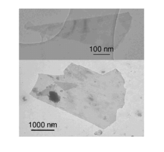
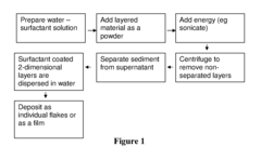
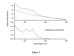
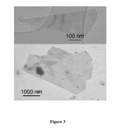
Process to Produce Atomically Thin Crystals and Films
PatentInactiveUS20130302593A1
Innovation
- A process involving mixing layered materials in a water-surfactant solution, applying energy through ultrasound, and centrifugal force to produce 2-dimensional crystals without altering their structural or material properties, using benign and non-combustible materials, allowing for ambient condition processing and scalable industrial production.
Quantum Security and Cryptography Standards
The evolution of quantum computing poses significant challenges to traditional cryptographic systems, necessitating the development of quantum-resistant security standards. Current public key infrastructures based on RSA and ECC algorithms are vulnerable to quantum attacks using Shor's algorithm, creating an urgent need for quantum-secure alternatives. Organizations like NIST have been actively developing post-quantum cryptography (PQC) standards, with their first selections announced in 2022, including CRYSTALS-Kyber for key establishment and CRYSTALS-Dilithium, FALCON, and SPHINCS+ for digital signatures.
TMD-based single-photon emitters offer promising applications within quantum cryptography protocols, particularly for quantum key distribution (QKD). These emitters can generate the non-classical light states required for BB84, E91, and other QKD protocols, potentially enabling unconditionally secure communication channels. The integration of TMD quantum emitters with existing fiber optic infrastructure represents a significant advantage for practical implementation.
International standardization efforts for quantum cryptography are progressing through multiple channels. The ETSI Quantum Safe Cryptography working group has published specifications for quantum-safe algorithmic frameworks. Similarly, ISO/IEC JTC 1/SC 27 is developing standards for quantum-resistant cryptographic primitives, while the ITU-T Focus Group on Quantum Information Technology for Networks has established recommendations for quantum key distribution networks.
Regulatory frameworks are also evolving to address quantum security concerns. The U.S. National Quantum Initiative Act and the EU's Quantum Flagship program both emphasize the importance of quantum-secure communications. Additionally, the Quantum Alliance Initiative has proposed QKD and QRNG standards to facilitate commercial adoption of quantum security technologies.
For TMD-based quantum emitters to be incorporated into quantum security standards, several technical challenges must be addressed. These include improving room-temperature operation stability, enhancing photon indistinguishability, and developing scalable fabrication processes. Certification methodologies for quantum random number generators and single-photon sources must also be established to ensure compliance with emerging standards.
The transition to quantum-secure cryptographic systems will likely follow a hybrid approach, where classical and post-quantum algorithms operate in parallel during an extended migration period. This strategy allows organizations to maintain backward compatibility while gradually implementing quantum-resistant solutions. TMD-based technologies could play a crucial role in this transition, particularly for specialized high-security applications where quantum key distribution offers advantages over purely algorithmic approaches.
Scalability and Integration Prospects
The scalability and integration of TMD-based quantum emitters represent critical factors for their practical implementation in quantum communication networks. Current fabrication methods for TMD quantum emitters face significant challenges when transitioning from laboratory demonstrations to industrial-scale production. The primary obstacle lies in achieving consistent quality and performance across large numbers of emitters, as variations in strain, defect concentration, and layer thickness can dramatically affect emission properties.
Integration with existing photonic platforms presents both opportunities and challenges. Silicon photonics offers a mature infrastructure for integrating TMD quantum emitters, potentially enabling on-chip quantum communication systems. Recent advances have demonstrated successful coupling of TMD emitters with silicon waveguides, achieving coupling efficiencies of up to 40%. However, maintaining quantum coherence during this integration process remains problematic due to environmental interactions that can degrade the single-photon purity.
Wafer-scale production techniques are emerging as promising approaches for scaling TMD quantum emitter fabrication. Chemical vapor deposition (CVD) methods can now produce relatively uniform TMD monolayers across 4-inch wafers, though the controlled introduction of quantum emitting sites at predetermined locations continues to be challenging. Deterministic transfer techniques using micromanipulators have shown promise for precise placement but lack the throughput necessary for large-scale applications.
Temperature stability represents another critical consideration for practical deployment. While most laboratory demonstrations operate at cryogenic temperatures (typically 4-10K), recent developments in strain engineering and defect management have pushed operating temperatures up to 77K, with some reports claiming room-temperature single-photon emission, albeit with reduced quantum efficiency and increased linewidth.
The economic viability of TMD quantum emitters depends on developing cost-effective fabrication methods that maintain quantum performance. Current estimates suggest that the cost per functional quantum emitter needs to decrease by approximately two orders of magnitude to compete with alternative technologies. This necessitates innovations in both materials synthesis and integration techniques, potentially leveraging existing semiconductor manufacturing infrastructure to reduce production costs.
Standardization efforts are beginning to emerge, with several research consortia working to establish benchmarks for TMD quantum emitter performance, including metrics for single-photon purity, indistinguishability, and operational stability. These standards will be essential for enabling interoperability in future quantum communication networks that may incorporate diverse quantum emitter technologies.
Unlock deeper insights with Patsnap Eureka Quick Research — get a full tech report to explore trends and direct your research. Try now!
Generate Your Research Report Instantly with AI Agent
Supercharge your innovation with Patsnap Eureka AI Agent Platform!