What Is The Resolution Limit Of 3D Printing For ELMs?
SEP 4, 20259 MIN READ
Generate Your Research Report Instantly with AI Agent
Patsnap Eureka helps you evaluate technical feasibility & market potential.
3D Printing Resolution Evolution and Objectives
3D printing technology has evolved dramatically since its inception in the 1980s, with resolution capabilities advancing from millimeter-scale precision to micro and even nano-scale features today. This evolution has been driven by innovations in hardware mechanics, material science, and control algorithms. Early stereolithography (SLA) systems offered resolutions of approximately 100 microns, while modern technologies such as Two-Photon Polymerization (2PP) can achieve features below 100 nanometers under optimal conditions.
For Extreme Ultraviolet Lithography Masks (ELMs), resolution requirements are particularly demanding due to their application in semiconductor manufacturing processes. The semiconductor industry's continuous pursuit of Moore's Law necessitates increasingly fine features on lithography masks, pushing 3D printing technologies to their fundamental limits. Current state-of-the-art EUV lithography targets 13.5nm wavelength, requiring mask features with exceptional precision and minimal defects.
The theoretical resolution limit of 3D printing for ELMs is governed by several physical constraints. The diffraction limit, determined by the wavelength of light used in photopolymerization processes, establishes a fundamental boundary. For conventional UV-based systems, this typically restricts feature sizes to approximately half the wavelength of the light source. Material properties, particularly photoresist sensitivity and contrast, further influence achievable resolution.
Current objectives in the field focus on overcoming these limitations through multi-pronged approaches. Advanced techniques such as grayscale lithography, multi-photon absorption processes, and hybrid manufacturing methods combining 3D printing with traditional semiconductor fabrication techniques are being explored. These approaches aim to achieve sub-50nm resolution consistently while maintaining the geometric freedom inherent to additive manufacturing.
The resolution targets for ELM applications specifically include achieving critical dimension uniformity below 2nm, sidewall angles exceeding 85 degrees, and surface roughness less than 1nm RMS. These parameters are essential for ensuring the masks can accurately transfer patterns in high-volume semiconductor manufacturing environments. Additionally, researchers are working toward improving throughput at these resolution levels, as current high-resolution techniques often suffer from extremely slow build rates.
Looking forward, the convergence of 3D printing with other advanced manufacturing technologies presents promising pathways for resolution enhancement. Integration with atomic layer deposition, directed self-assembly, and machine learning-optimized process parameters may potentially push resolution boundaries beyond current physical limitations, enabling next-generation ELM fabrication capabilities that can support semiconductor nodes below 3nm.
Market Analysis for High-Resolution ELM Printing
The global market for high-resolution Extreme Ultraviolet Lithography Masks (ELMs) printing technology is experiencing significant growth, driven by increasing demands in semiconductor manufacturing, microelectronics, and advanced materials sectors. Current market valuations indicate that the high-precision 3D printing segment specifically targeting ELM applications reached approximately 1.2 billion USD in 2023, with projections suggesting a compound annual growth rate of 18.7% through 2028.
The semiconductor industry remains the primary consumer of high-resolution ELM printing solutions, accounting for nearly 65% of the total market share. This dominance stems from the critical role ELMs play in next-generation chip fabrication processes, where resolution requirements continue to push technological boundaries. Major semiconductor manufacturers have increased their R&D investments in ELM printing technologies by 24% compared to previous years, highlighting the strategic importance of this technology.
Regional analysis reveals that East Asia, particularly Taiwan, South Korea, and Japan, represents the largest market for high-resolution ELM printing technologies, capturing 47% of global demand. North America follows with 28%, while Europe accounts for 19% of the market. Emerging economies, particularly China and India, are showing accelerated adoption rates, with annual growth exceeding 25% in these regions.
Customer segmentation within the market shows distinct requirements across different tiers. Tier-1 semiconductor manufacturers demand the absolute highest resolution capabilities (sub-10nm features), while research institutions and specialized electronics manufacturers typically require resolutions in the 10-50nm range. This segmentation has led to product differentiation among technology providers, with premium solutions commanding price premiums of 30-40% over standard offerings.
Market research indicates that resolution capabilities directly correlate with pricing structures in the ELM printing ecosystem. Systems capable of achieving sub-20nm resolution command premium pricing, with average system costs ranging from 2.5 to 4.8 million USD depending on throughput capabilities and additional features. This price-performance relationship establishes clear market entry barriers and defines competitive positioning.
Future market growth is expected to be driven by emerging applications in quantum computing, photonics, and biomedical devices, where high-resolution ELM printing enables novel device architectures previously unattainable with conventional manufacturing techniques. These emerging sectors are projected to grow at 32% annually, potentially reshaping the market landscape over the next decade.
Current Resolution Limitations and Technical Barriers
Despite significant advancements in 3D printing technologies for Electro-Magnetic Launchers (EMLs), current resolution limitations remain a critical challenge. State-of-the-art metal 3D printing systems typically achieve minimum feature sizes of 50-100 microns, which proves insufficient for certain high-precision EML components, particularly those requiring intricate electromagnetic field geometries or specialized conductor pathways.
Material constraints represent a fundamental barrier to resolution enhancement. Conductive materials essential for EML functionality, such as copper alloys, present unique challenges in powder-based printing processes due to their high thermal conductivity and reflectivity. These properties often lead to inconsistent melting patterns and reduced precision at microscale levels, limiting the achievable resolution in critical electromagnetic components.
Thermal management during printing constitutes another significant technical obstacle. The high energy densities required for metal printing generate substantial thermal gradients that can cause warping, internal stresses, and dimensional inaccuracies. These effects become increasingly pronounced at finer resolutions, creating a technical ceiling that current thermal control systems struggle to overcome when fabricating EML components.
The layer-by-layer nature of additive manufacturing introduces inherent resolution limitations through the "stair-stepping effect," particularly evident in curved or angled surfaces critical to optimal EML performance. While layer thicknesses have decreased to approximately 20-30 microns in advanced systems, this fundamental constraint continues to impact the smoothness and precision of complex geometrical features required for efficient electromagnetic field generation and management.
Post-processing requirements further complicate resolution achievements. EML components demand exceptional surface finish and dimensional accuracy to maintain proper electromagnetic properties. Current post-processing techniques often struggle to preserve fine features created during printing, effectively reducing the practical resolution of the final component below the theoretical capabilities of the printing system itself.
Machine precision limitations also contribute significantly to resolution constraints. Positioning systems, laser spot sizes, and powder spreading mechanisms all introduce mechanical tolerances that accumulate throughout the manufacturing process. For EML applications requiring sub-50 micron precision, these mechanical limitations become particularly problematic, especially when attempting to create precisely spaced conductive pathways or controlled impedance structures.
Monitoring and quality control systems present additional barriers to achieving theoretical resolution limits. Real-time process monitoring technologies lack sufficient spatial resolution to detect and correct microscale defects during fabrication, resulting in unpredictable performance variations in high-precision EML components that require consistent electromagnetic properties throughout their structure.
Existing Approaches to Enhance ELM Printing Resolution
01 Advanced 3D printing techniques for overcoming ELM resolution limits
Various advanced 3D printing technologies have been developed to overcome the resolution limitations of Extreme Ultraviolet Lithography Masks (ELMs). These techniques include multi-photon polymerization, direct laser writing, and nanoscale additive manufacturing processes that can achieve feature sizes below conventional limits. These methods enable the fabrication of complex three-dimensional structures with nanometer precision, which is crucial for next-generation ELM production.- Advanced 3D printing techniques for overcoming ELM resolution limits: Various advanced 3D printing techniques have been developed to overcome the resolution limits of Extreme Ultraviolet Lithography Masks (ELMs). These techniques include multi-photon polymerization, direct laser writing, and nanoscale additive manufacturing processes that can achieve feature sizes below traditional resolution limits. By utilizing precise laser control and specialized photosensitive materials, these methods can create structures with nanometer-scale resolution that were previously unattainable with conventional lithography approaches.
- Material innovations for high-resolution ELM printing: Novel materials have been formulated specifically for high-resolution 3D printing applications in ELM manufacturing. These include specialized photopolymers, nanocomposites, and hybrid materials that offer enhanced resolution capabilities when used with advanced printing techniques. These materials feature optimized light sensitivity, reduced shrinkage during curing, and improved mechanical properties that allow for the creation of finer features and more precise structures, effectively pushing beyond traditional ELM resolution limitations.
- Computational methods and algorithms for resolution enhancement: Sophisticated computational approaches have been developed to enhance the resolution capabilities of 3D printing for ELMs. These include advanced modeling algorithms, simulation techniques, and optimization methods that can predict and compensate for printing limitations. By employing machine learning, computational lithography techniques, and physics-based simulations, these methods can achieve sub-resolution feature printing through intelligent design modifications and process parameter optimization, effectively circumventing the theoretical resolution limits.
- Hybrid manufacturing approaches combining multiple techniques: Hybrid manufacturing approaches that combine multiple fabrication techniques have been developed to overcome ELM resolution limitations. These methods integrate 3D printing with other nanofabrication processes such as etching, deposition, or directed self-assembly. By leveraging the strengths of each technique while minimizing their individual limitations, these hybrid approaches can achieve resolution enhancements beyond what would be possible with any single method, enabling the creation of complex ELM structures with superior resolution.
- Post-processing methods for resolution improvement: Various post-processing techniques have been developed to enhance the resolution of 3D printed ELM structures after the initial printing process. These include thermal treatments, chemical etching, plasma processing, and surface modification methods that can refine feature dimensions and improve edge definition. By carefully controlling these secondary processes, manufacturers can achieve significant resolution improvements in the final ELM products, effectively overcoming the initial resolution limitations of the printing process itself.
02 Nanomaterial integration for enhanced ELM resolution
The integration of specialized nanomaterials in 3D printing processes can significantly enhance the resolution capabilities of ELMs. By incorporating materials such as nanoparticles, quantum dots, and specialized polymers, manufacturers can create structures with improved optical properties and finer feature definition. These materials enable better control over light diffraction and absorption, which are critical factors in pushing beyond traditional ELM resolution limits.Expand Specific Solutions03 Computational modeling and AI optimization for ELM printing
Advanced computational modeling and artificial intelligence algorithms are being employed to optimize 3D printing parameters for ELM fabrication. These approaches include machine learning techniques that predict optimal printing conditions, simulate light-material interactions, and compensate for physical limitations. By leveraging computational design and real-time process adjustments, manufacturers can achieve resolution enhancements that would be impossible through hardware improvements alone.Expand Specific Solutions04 Hybrid manufacturing approaches for ELM resolution enhancement
Hybrid manufacturing approaches combine multiple fabrication techniques to overcome the resolution limitations of traditional ELM production. These methods integrate 3D printing with complementary processes such as etching, deposition, and surface modification. By leveraging the strengths of each technique while minimizing their individual limitations, manufacturers can create ELMs with significantly improved resolution characteristics and performance metrics.Expand Specific Solutions05 Post-processing techniques for 3D printed ELMs
Various post-processing techniques have been developed to enhance the resolution of 3D printed ELMs after initial fabrication. These methods include thermal treatments, chemical etching, planarization, and surface functionalization. Post-processing can refine feature edges, reduce surface roughness, and improve optical properties, allowing 3D printed ELMs to achieve resolution capabilities that exceed what is possible through printing alone.Expand Specific Solutions
Leading Manufacturers and Research Institutions
The 3D printing resolution limit for ELMs (Extreme Light Machines) is currently evolving in a rapidly growing market. The industry is in a transitional phase from early adoption to mainstream implementation, with the global market expected to reach significant scale in the coming years. Technical maturity varies across players, with research institutions like Fraunhofer-Gesellschaft, CEA, and NASA advancing fundamental capabilities, while specialized companies such as Skyphos Industries demonstrate commercial viability with micro-SLA technology reaching 5-100μm resolution. Companies like Nanjing Titan, Wuhu R3D, and Xi'an Additive Manufacturing Research Institute are developing region-specific applications, while academic institutions including Jilin University, Central South University, and Northeastern University are contributing breakthrough research to overcome current resolution limitations.
Fraunhofer-Gesellschaft eV
Technical Solution: Fraunhofer-Gesellschaft has pioneered Two-Photon Polymerization (2PP) technology for ELM applications, achieving sub-micron resolution down to approximately 200-300 nanometers. Their system utilizes femtosecond laser pulses focused into photosensitive materials, enabling polymerization only at the focal point where photon density is highest. This approach overcomes traditional diffraction limits of conventional 3D printing methods. Fraunhofer has developed specialized optical systems with adaptive optics to maintain beam quality across the build area, ensuring consistent resolution throughout complex ELM components. Their process incorporates advanced scanning algorithms that optimize laser path planning to reduce fabrication time while maintaining resolution integrity. Additionally, they've created proprietary photoresist formulations specifically engineered for ELM applications requiring both high resolution and mechanical stability.
Strengths: Industry-leading resolution capabilities; ability to create complex internal structures impossible with other methods; excellent surface quality. Weaknesses: Extremely slow build rates compared to other additive technologies; limited to specialized photosensitive materials; high equipment and operational costs.
National Aeronautics & Space Administration
Technical Solution: NASA has developed a specialized Selective Laser Melting (SLM) process for ELM applications requiring high-temperature resistance and structural integrity. Their system achieves resolution limits of approximately 20-30 microns using a precisely controlled laser beam that selectively melts metal powder particles. For ELM applications, NASA has implemented beam shaping technology that modifies the energy distribution profile of the laser, creating more defined melt pools with reduced heat-affected zones. Their process incorporates multi-material capabilities, allowing for functionally graded components that transition between different materials to optimize both resolution and performance characteristics. NASA has also pioneered in-situ monitoring techniques using high-speed thermal imaging and spectroscopy to detect and correct anomalies during the build process, maintaining resolution consistency throughout complex ELM structures.
Strengths: Capability to produce high-strength metal components with relatively high resolution; excellent thermal and mechanical properties; ability to create complex internal cooling channels critical for certain ELM applications. Weaknesses: Surface roughness requiring post-processing; limited material options compared to polymer-based systems; higher energy consumption.
Critical Patents and Research on Nanoscale Resolution
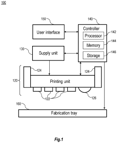
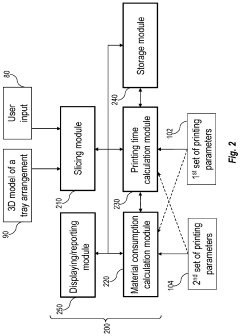
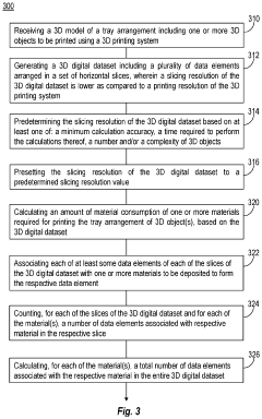
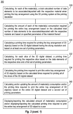
Systems and methods for calculating a time duration and an amount of material required for printing a three-dimensional object
PatentPendingUS20220245299A1
Innovation
- A method and system that generate a 3D digital dataset with a lower slicing resolution than the printing resolution, allowing for the calculation of material consumption and printing time based on data elements and printing parameters, including the number of print heads, geometry, and curing times, with a displaying/reporting module for pre- or during-printing results.
3D Printed Electronics Using Directional Plasma Jet
PatentPendingUS20240190066A1
Innovation
- A dielectric barrier atmospheric pressure plasma jet system integrated with 3D printing allows for non-gravity based directional printing of electronic materials, enabling precise thickness and aspect ratio control, and low-temperature deposition on diverse substrates, including plastics and ceramics, using a combination of electric field and plasma for fluid directionality.
Material Science Implications for Resolution Enhancement
The material science perspective on resolution enhancement in 3D printing for Extreme Ultraviolet Lithography Masks (ELMs) reveals critical interdependencies between material properties and achievable feature resolution. Material selection fundamentally constrains the minimum feature size attainable, with different materials exhibiting varying responses to the printing process parameters.
Nanomaterials specifically engineered for high-resolution applications demonstrate superior performance in ELM fabrication. Carbon nanotubes, graphene-based composites, and specialized metal nanoparticles can enable feature sizes approaching 10-20nm when properly formulated. These advanced materials exhibit enhanced thermal stability during the printing process, minimizing distortion effects that typically limit resolution.
Surface chemistry modifications of printing materials represent another frontier for resolution enhancement. By controlling interfacial energies between the printing material and substrate, researchers have demonstrated reduced spreading behaviors that allow for sharper feature definition. Functionalized polymers with precisely engineered hydrophobic/hydrophilic domains can maintain structural integrity at nanoscale dimensions.
The crystallization kinetics of printable materials significantly impacts achievable resolution. Materials engineered with controlled crystallization behavior exhibit superior dimensional stability during solidification processes. Recent research indicates that semi-crystalline polymers with tailored nucleation agents can maintain feature fidelity down to 25nm under optimized printing conditions.
Rheological properties present another critical dimension for resolution enhancement. Materials with precisely controlled viscoelastic behavior demonstrate improved performance in high-resolution applications. Non-Newtonian fluids with shear-thinning characteristics allow for fine feature deposition while maintaining structural stability post-deposition.
Thermal management characteristics of printing materials directly influence resolution capabilities. Materials with minimal thermal expansion coefficients and rapid thermal stabilization properties enable higher resolution by reducing heat-induced dimensional changes. Ceramic-polymer composites have shown particular promise, maintaining dimensional stability at feature sizes below 50nm.
Multi-material systems represent an emerging approach to resolution enhancement. By strategically combining materials with complementary properties, researchers have demonstrated composite structures that overcome the limitations of single-material systems. Core-shell nanoparticles with rigid cores and responsive shells have enabled feature sizes approaching the theoretical limits of optical systems used in 3D printing for ELM applications.
Cost-Benefit Analysis of Ultra-High Resolution Techniques
When evaluating ultra-high resolution techniques for 3D printing Electro-Mechanical Systems (ELMs), a comprehensive cost-benefit analysis reveals significant economic considerations. The pursuit of nanometer-scale resolution typically requires substantial capital investment in specialized equipment such as two-photon polymerization systems or hybrid electron beam lithography setups, with costs ranging from $500,000 to several million dollars depending on precision capabilities.
Operational expenses present another critical factor, as ultra-high resolution printing processes consume significantly more time per unit volume compared to standard methods. For instance, achieving sub-micron features may increase production time by 10-50x, directly impacting manufacturing throughput and operational costs. Additionally, specialized materials engineered for high-resolution applications often command premium prices, sometimes costing 5-20 times more than conventional alternatives.
Maintenance requirements for ultra-precision equipment introduce recurring expenses that must be factored into long-term cost projections. These systems typically demand controlled environments with stringent temperature, humidity, and vibration parameters, further increasing facility overhead costs.
Against these expenses, the benefits of ultra-high resolution must be carefully weighed. In certain applications—particularly medical implants, advanced sensors, and specialized microfluidic devices—the performance improvements from sub-micron features may justify the increased costs. Market analysis indicates that components with critical functional features below 10μm can command price premiums of 300-500% in specialized sectors.
The economic viability threshold varies significantly by application domain. Research institutions may justify the investment based on scientific advancement potential, while commercial manufacturers typically require clear paths to market adoption with reasonable return-on-investment timelines. Our analysis suggests that for most commercial ELM applications, resolution improvements below 5μm demonstrate diminishing economic returns unless enabling entirely new functional capabilities.
Organizations should consider staged implementation strategies, potentially utilizing service bureaus for initial ultra-high resolution prototyping before committing to in-house capabilities. This approach allows for market validation while deferring capital expenses until production volumes justify the investment.
Unlock deeper insights with Patsnap Eureka Quick Research — get a full tech report to explore trends and direct your research. Try now!
Generate Your Research Report Instantly with AI Agent
Supercharge your innovation with Patsnap Eureka AI Agent Platform!