Packaging method for small-size PCBs

A technology of PCB board and packaging method, applied in the field of packaging of small-sized PCB boards, can solve the problems of skew, moving scratches, defects, etc., and achieve the effect of simple and fast packaging problems, safe and reliable packaging problems

Inactive Publication Date: 2016-06-08
SHENZHEN KINWONG ELECTRONICS
View PDF6 Cites 5 Cited by
  • Summary
  • Abstract
  • Description
  • Claims
  • Application Information

AI Technical Summary

Problems solved by technology

[0004] In view of the above-mentioned deficiencies in the prior art, the purpose of the present invention is to provide a packaging method for small-sized PCB boa

Method used


Image

  • Packaging method for small-size PCBs
  • Packaging method for small-size PCBs

Examples


Embodiment Construction

[0019] The present invention provides a packaging method for small-sized PCB boards. In order to make the purpose, technical solution and effect of the present invention clearer and clearer, the present invention will be further described in detail below. It should be understood that the specific embodiments described here are only used to explain the present invention, not to limit the present invention.

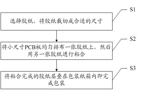
[0020] see figure 1 , figure 1 It is a flow chart of a preferred embodiment of a packaging method for a small-size PCB board of the present invention, as shown in the figure, which includes steps:

[0021] S1. Select the adhesive tape, and cut the adhesive tape into a suitable size;

[0022] S2. Evenly arrange the small-sized PCB boards on a piece of adhesive paper, and then use another piece of adhesive paper to bond them;

[0023] S3. Laminating the glued tapes in the packaging carton to complete the packaging.

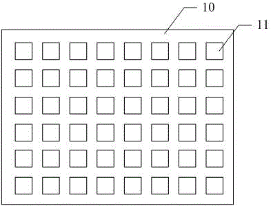
[0024] In the present invention, if figure 2 As shown...


PUM

PropertyMeasurementUnit
Sizeaaaaaaaaaa

Abstract

The invention discloses a packaging method for small-size PCBs. The packaging method includes the steps that gummed paper is selected and cut into the proper size; the small-size PCBs are uniformly distributed on the gummed paper, and then another gummed paper and the gummed paper are bonded; and the bonded gummed paper is overlaid in a packaging carton, and therefore packaging is completed. The problems that the small-size PCBs are prone to moving, collapsing and skewing in the packaging process are solved, or complex packaging methods for solving the problems are avoided, for example, special clamps and special packaging boxes are omitted. By means of the packaging method, the packaging problems of the small-size PCBs can be solved simply, quickly, safely and reliably.

Description

technical field [0001] The invention relates to the field of PCB packaging, in particular to a packaging method for small-sized PCB boards. Background technique [0002] After the PCB production is completed, the usual shipping method is continuous shipment, but for small-sized PCB boards that do not accept continuous shipment, it is prone to poor scratches caused by collapse, skew, movement, etc. during the packaging process Phenomenon. [0003] Therefore, the prior art still needs to be improved and developed. Contents of the invention [0004] In view of the above-mentioned deficiencies in the prior art, the purpose of the present invention is to provide a packaging method for small-sized PCB boards, aiming to solve the poor scratches caused by the collapse, skew, movement, etc. of the existing small-sized PCB boards during the packaging process. question. [0005] Technical scheme of the present invention is as follows: [0006] A kind of packing method of small-si...

Claims


Application Information

Patent Timeline
IPC IPC(8): B65B15/02B65B5/10
CPCB65B15/02B65B5/10
Inventor 吴正根王俊马奕
Owner SHENZHEN KINWONG ELECTRONICS
Why Eureka
Try Eureka