Circuit board chip burning method and device, terminal and computer readable storage medium

A programming method and circuit board technology, applied in software deployment and other directions, can solve the problems of easy error, low efficiency, high labor intensity, etc., to reduce labor intensity, improve programming efficiency, and avoid programming errors.

Pending Publication Date: 2020-08-07
GUANGZHOU HUIRUI SITONG INFORMATION SCI & TECH CO LTD
View PDF5 Cites 5 Cited by
  • Summary
  • Abstract
  • Description
  • Claims
  • Application Information

AI Technical Summary

Problems solved by technology

[0003] In order to solve the problems of high labor intensity, low efficiency, and error-prone problems caused by manual operation during the above-mentioned chip programming, the embodiment of the present invention provides a circuit board chip programming method, device, terminal and computer-readable storage medium

Method used


Image

  • Circuit board chip burning method and device, terminal and computer readable storage medium
  • Circuit board chip burning method and device, terminal and computer readable storage medium
  • Circuit board chip burning method and device, terminal and computer readable storage medium

Examples


Embodiment Construction

[0044] In order to make the purpose, technical solutions and advantages of the embodiments of the present invention clearer, the technical solutions in the embodiments of the present invention will be clearly and completely described below in conjunction with the drawings in the embodiments of the present invention. Obviously, the described embodiments It is a part of embodiments of the present invention, but not all embodiments. Based on the embodiments of the present invention, all other embodiments obtained by persons of ordinary skill in the art without making creative efforts belong to the protection scope of the present invention.

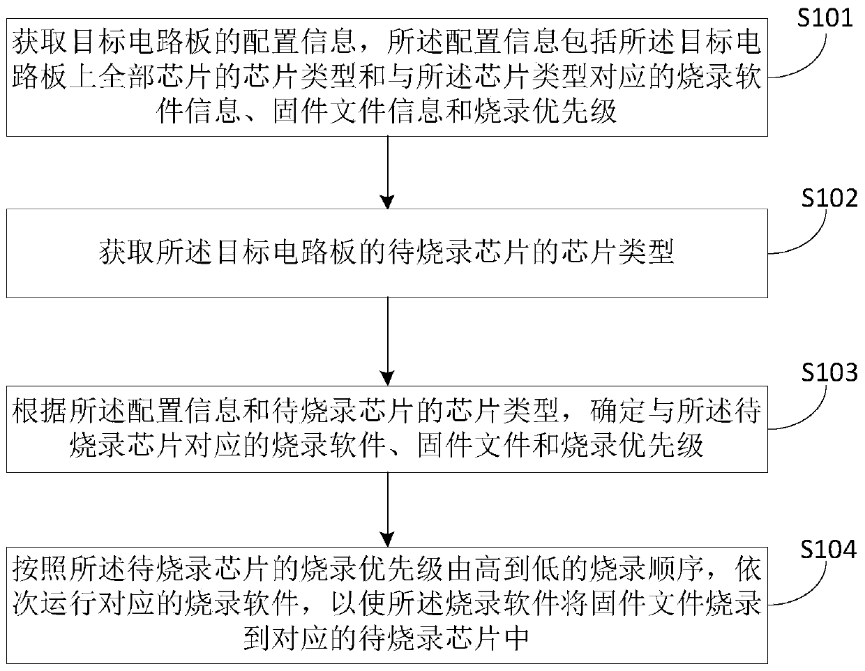
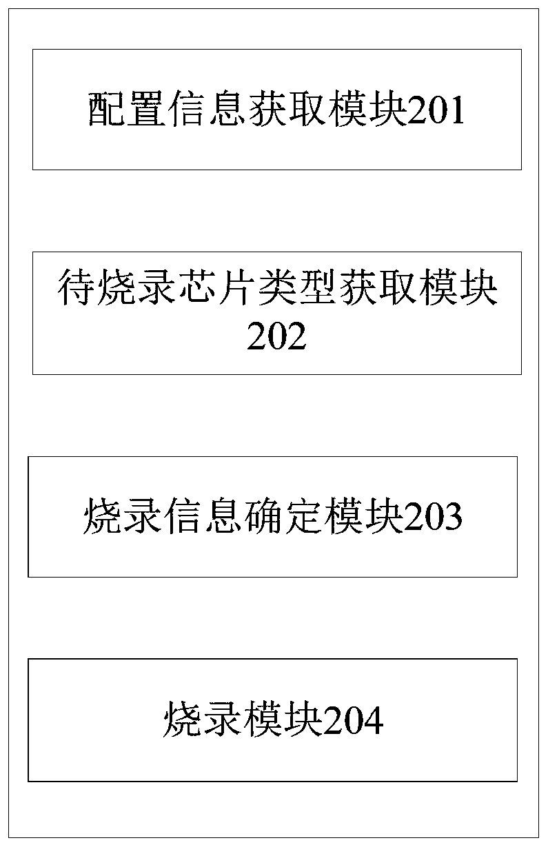
[0045] figure 1 The embodiment of the present invention provides the flow chart of a kind of circuit board chip burning method, and this circuit board chip burning method can be used for at least two kinds of chip type chips (for example ARM chip, Ti company chip and Altera chip) of soldering on the circuit board company chip, etc.) for auto...


PUM


Abstract

The embodiment of the invention provides a circuit board chip burning method and device, a terminal and a computer readable storage medium. The method comprises the steps of obtaining a configurationfile of a target circuit board; acquiring the chip types of all chips welded on the target circuit board, and burning software information, firmware file information and burning priorities corresponding to the chip types at one time; obtaining a chip type of a to-be-burnt chip, directly obtaining burning software information, firmware file information and burning priorities corresponding to the chip types of the chips to be burnt from the configuration file, determining a burning sequence of the chips to be burnt according to the burning priorities, sequentially running the corresponding burning software according to the burning sequence, and burning the corresponding firmware files into the corresponding chips to be burnt. According to the circuit board chip burning method provided by theinvention, at least two different types of chips in one target circuit board can be automatically burnt, the burning efficiency is improved, the labor intensity is reduced, and burning errors can beavoided.

Description

technical field [0001] The embodiments of the present invention relate to the technical field of chip programming, and in particular to a circuit board chip programming method, device, terminal, and computer-readable storage medium. Background technique [0002] Most of the controllers used in modern electronic technology are programmable chips. Before using a programmable chip to realize a certain function, it is necessary to burn specific program codes for the programmable chip. These program codes can be called firmware files. In the prior art, specific chips are mostly programmed through proprietary programming software, but one programming software cannot take into account the programming of multiple chips. For example, the ARM J-Link programming software can only program ARM chips. , the Ti Fusion burning software can only burn the chips of Ti Company, and the Quartus burning software can only burn the chips of Altera Company. A target circuit board with chips of diff...

Claims


Application Information

Patent Timeline
Patent Type & Authority Applications(China)
IPC IPC(8): G06F8/61
CPCG06F8/63
Inventor 李健强
Owner GUANGZHOU HUIRUI SITONG INFORMATION SCI & TECH CO LTD
Why Eureka
Try Eureka