
Novel distributed array and contact architecture for 4-stacked 3d X point memory
A memory and contact technology, applied in the field of three-dimensional electronic memory, can solve problems such as high cost
Patent Information
- Authority / Receiving Office
- CN · China
- Patent Type
- Patents(China)
- Current Assignee / Owner
- Publication Date
- 2022-04-22
Smart Images
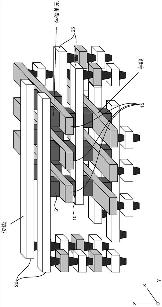
Figure 1 
Figure 2 
Figure 3
Abstract
Description
technical field
[0001] In general, the present disclosure relates to three-dimensional electronic memory, and in particular, the present disclosure relates to increasing the density of memory cells in three-dimensional cross-point (X-point) memory. Background technique
[0002] Planar memory cells are shrunk to smaller sizes by improving process technology, circuit design, programming algorithms, and manufacturing processes. However, as the feature size of memory cells approaches the lower limit, planar processes and fabrication techniques become challenging and costly. Therefore, the storage density of planar memory cells approaches the upper limit. There remains a need for three-dimensional (3D) memory architectures that can address the density limitations in planar memory cells. Contents of the invention
[0003] The three-dimensional memory and methods disclosed herein solve the problems of the state of the art and provide additional benefits. According to one aspec...
Examples
Embodiment Construction
[0015] The technology is applied in the field of three-dimensional memory. exist figure 1 A general example of a three-dimensional (3D) memory is shown in . in particular, figure 1 is a perspective view of a portion of a three-dimensional intersection memory. The memory includes a first layer storage unit 5 and a second layer storage unit 10 . Between the first layer memory cells 5 and the second layer memory cells 10 are a plurality of word lines 15 extending in the horizontal (X) direction. In the depth (Z) direction, a plurality of first bit lines 20 extending along the vertical (Y) direction are above the first layer of memory cells 5, and a plurality of first bit lines 20 extending along the Y direction are below the second layer of memory cells 10. A second bit line 25.
[0016] further as figure 1 As shown in , the sequential structure of bit line, memory cell, word line, memory cell can be repeated along the Z direction to form a stacked configuration. exist fi...