Array substrate, display device and method for fabricating array substrate

a technology which is applied in the field of array substrate and display device, can solve the problems of small bright spot and consequently affect and achieve the effect of improving the display quality of the display device and easy short circui

Active Publication Date: 2017-03-07
TCL CHINA STAR OPTOELECTRONICS TECH CO LTD
View PDF3 Cites 0 Cited by
  • Summary
  • Abstract
  • Description
  • Claims
  • Application Information

AI Technical Summary

Benefits of technology

[0006]The invention provides an array substrate, and the array substrate can achieve high display quality.
[0017]In the array substrate and the display device of the invention, by adding the filling layer in the pull-down capacitor, the second conductive layer of the pull-down capacitor and the pixel electrode are arranged at different planes / levels, a distance between the second conductive layer and the pixel electrode are increased, and therefore the second conductive layer and the pixel electrode are not easy to be short-circuited, the display quality of the display device is improved consequently.

Problems solved by technology

In a fabricating process of the array substrate, such as etching or developing process, it is easy to produce residual transparent conductive layer, resulting in short circuit occurred between the transparent conductive layer as the topmost layer of the thin film transistor of the sub area (Sub TFT) and the transparent conductive layer as the topmost layer of the pull-down capacitor with the MII structure, the pull-down capacitor could not normally pull down the pixel voltage of the sub area, the pixel would produce a small bright spot and display quality of the display device is affected consequently.

Method used


Image

  • Array substrate, display device and method for fabricating array substrate
  • Array substrate, display device and method for fabricating array substrate
  • Array substrate, display device and method for fabricating array substrate

Examples


Embodiment Construction

[0024]In the following, with reference to accompanying drawings of embodiments of the invention, technical solutions in the embodiments of the invention will be clearly and completely described. Apparently, the embodiments of the invention described below only are a part of embodiments of the invention, but not all embodiments. Based on the described embodiments of the invention, all other embodiments obtained by ordinary skill in the art without creative effort belong to the scope of protection of the invention.

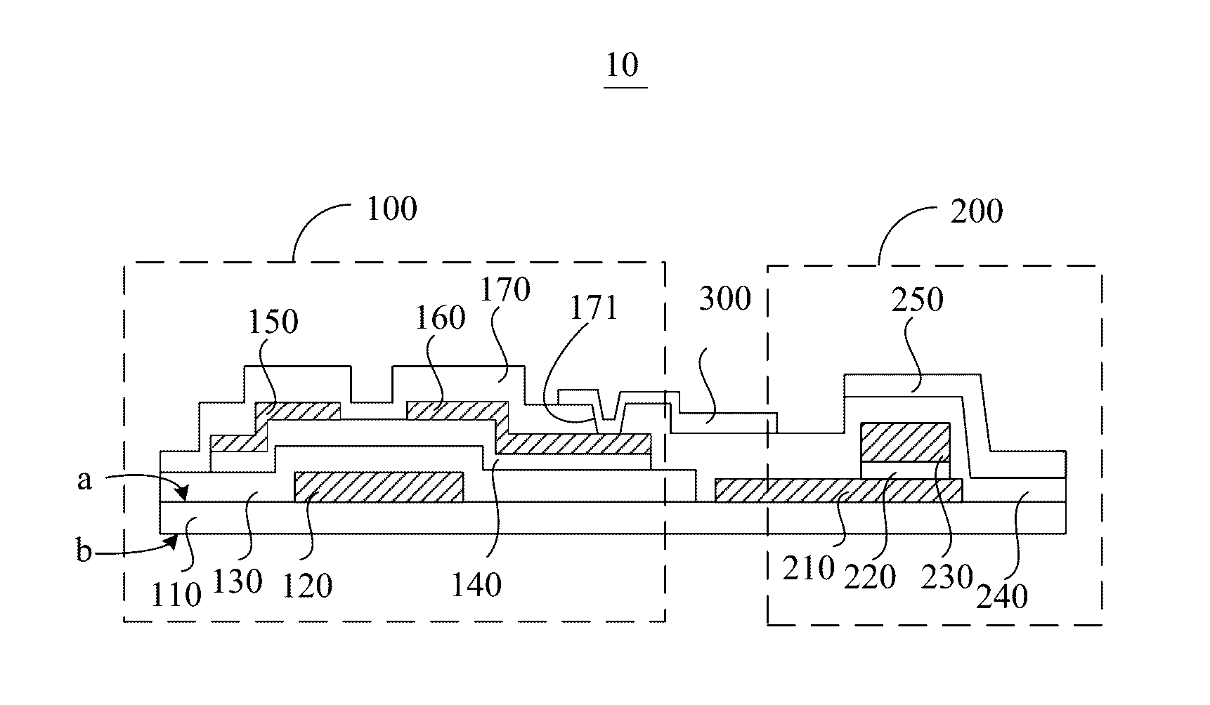
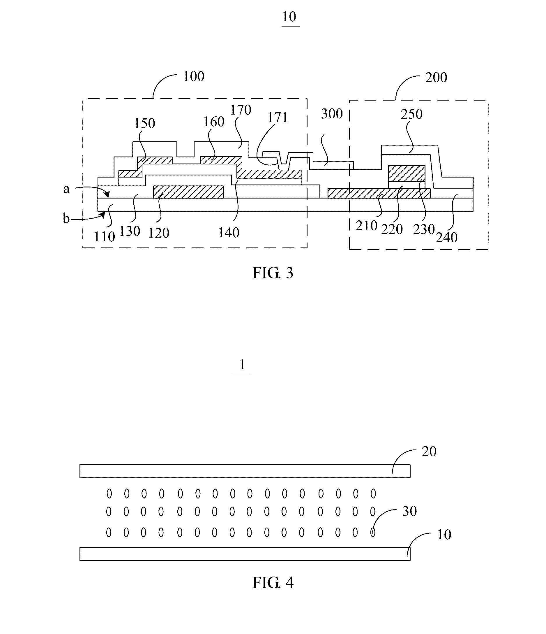
[0025]Please refer to FIG. 3, FIG. 3 is a schematic structural cross-sectional view of an array substrate according to a preferred embodiment of the invention. In particular, the array substrate 10 includes a substrate 110, and a thin film transistor 100 and a pull-down capacitor 200 disposed on a same side of the substrate 110. The thin film transistor 100 may be a thin film transistor corresponding to a sub pixel area, and the pull-down capacitor 200 is disposed neighborin...


PUM


Abstract

The invention provides an array substrate, a method therefor and a display device. The array substrate includes: a substrate, and a thin film transistor (TFT) and a pull-down capacitor disposed on the substrate. The TFT includes: a gate, a gate insulating layer, a channel layer, a source, a drain and a passivation layer. The passivation layer is disposed with a via hole corresponding to the drain, a pixel electrode is connected to the drain through the via hole. The pull-down capacitor includes: a first conductive layer, a first spacer layer, a filling layer, a second spacer layer and a second conductive layer successively stacked on the substrate. The sum of thicknesses of the filling layer and the first spacer layer is greater than the sum of thicknesses of the drain and the channel layer, to make the second conductive layer and the pixel electrode be located at different levels.

Description

CROSS REFERENCE TO RELATED APPLICATION[0001]This application claims the priority of Chinese Patent Application No. 201410855413.8 entitled “Array Substrate, Display Device and Method for Fabricating Array Substrate”, filed on Dec. 31, 2014, the disclosure of which is incorporated herein by reference in its entirety.BACKGROUND OF THE INVENTION[0002]1 . Field of the Invention[0003]The invention relates to the field of display technology, and particularly to an array substrate and a display device.[0004]2 . Description of Related Art[0005]A liquid crystal display (LCD) is a commonly used electronic device, and because of its low power consumption, small size, light weight and other characteristics, it is quite popular for users. In a thin film transistor liquid crystal display (TFT-LCD) employing a vertical alignment technology, a pixel generally is demarcated / divided into a main area and a sub area, and a pixel voltage applied onto the sub area is lower than a pixel voltage applied on...

Claims


Application Information

Patent Timeline
Patent Type & Authority Patents(United States)
IPC IPC(8): H01L27/12
CPCH01L27/1222H01L27/127H01L27/1248H01L27/1255H01L27/1259H01L27/1262
Inventor LIU, HUAN
Owner TCL CHINA STAR OPTOELECTRONICS TECH CO LTD
Why Eureka
Try Eureka