
Groove Gamma gate transistor with high electron mobility and preparing method thereof
A high electron mobility, transistor technology, applied in the field of microelectronics, can solve the problems of weakening the input and output isolation of the device, reducing the yield of the device, and reducing the stability of the device, so as to reduce the gate leakage current and improve the breakdown voltage. , the effect of large drain-source voltage
Patent Information
- Authority / Receiving Office
- CN · China
- Patent Type
- Patents(China)
- Current Assignee / Owner
- Publication Date
- 2010-08-11
- Estimated Expiration
- Not applicable · inactive patent
Smart Images

Figure 1 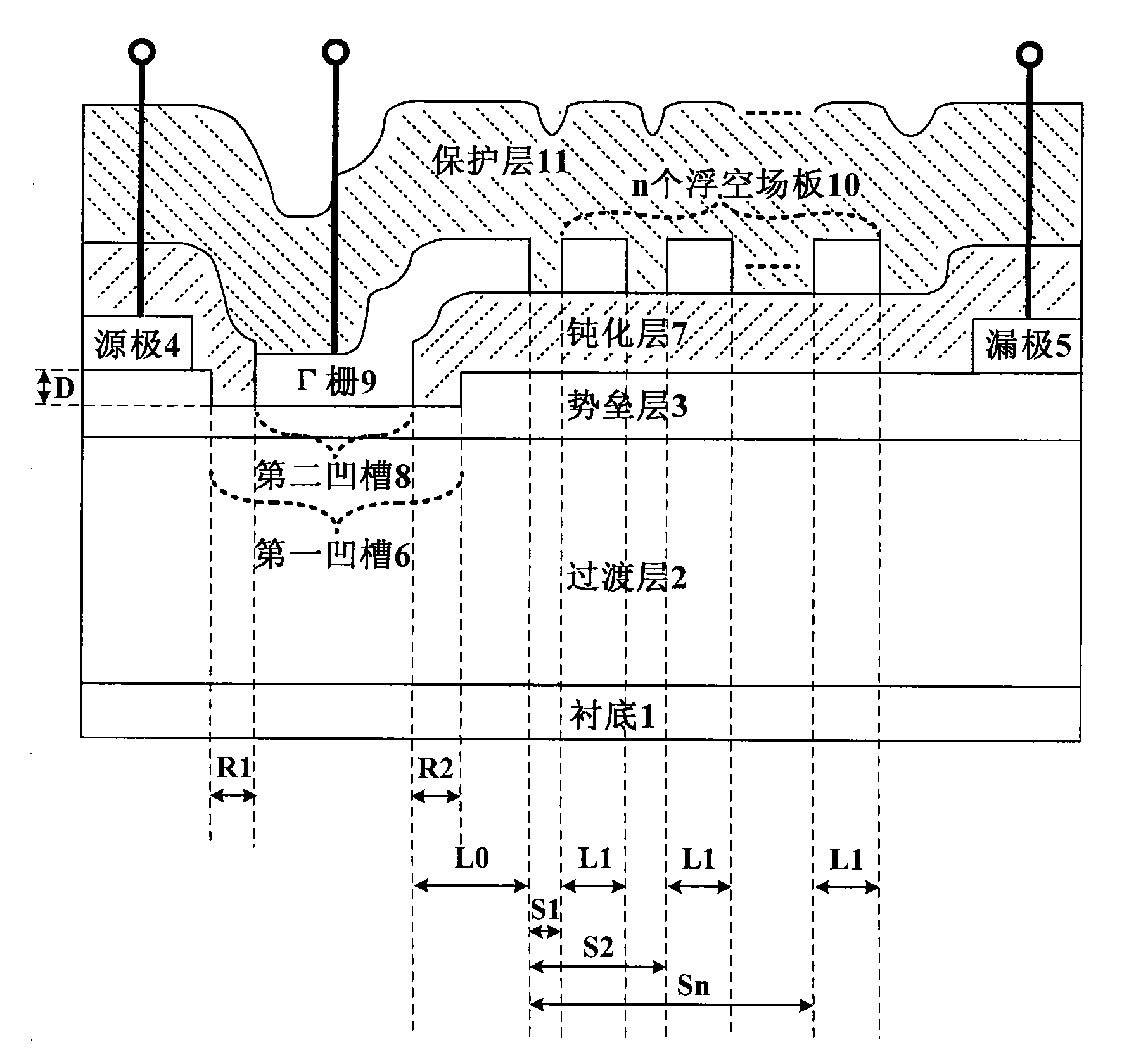
Figure 2 
Figure 3
Abstract
Description
technical field The invention belongs to the technical field of microelectronics, and relates to semiconductor devices, in particular to a grooved Γ-gate high electron mobility transistor based on the heterojunction structure of III-V compound semiconductor materials, which can be used as a microwave, millimeter wave communication system and radar system. basic device. technical background As is well known in the industry, semiconductor materials composed of group III elements and group V elements, that is, group III-V compound semiconductor materials, such as gallium nitride (GaN)-based, gallium arsenide (GaAs)-based, indium phosphide (InP)-based And other semiconductor materials, their bandgap widths are often quite different, so people usually use these III-V compound semiconductor materials to form various heterojunction structures. Due to the large difference in the band gap of III-V compound semiconductor materials on both sides of the heterojunction interface in the ...
Examples
Embodiment 1
Embodiment 2
Embodiment 3