
Optical input preamplifier for optical communication receiver
A preamplifier and receiver technology, applied in the field of optical communication reception, can solve the problems of difficult-to-burst signal reception amplification, response delay and low reception sensitivity, and achieve high open-loop gain and bandwidth, high optical reception sensitivity, and reduced response time. delayed effect
Patent Information
- Authority / Receiving Office
- CN · China
- Patent Type
- Patents(China)
- Current Assignee / Owner
- Publication Date
- 2011-06-15
- Estimated Expiration
- Not applicable · inactive patent
Smart Images
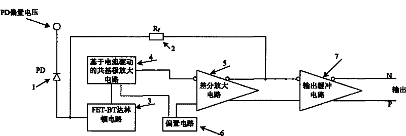
Figure 1 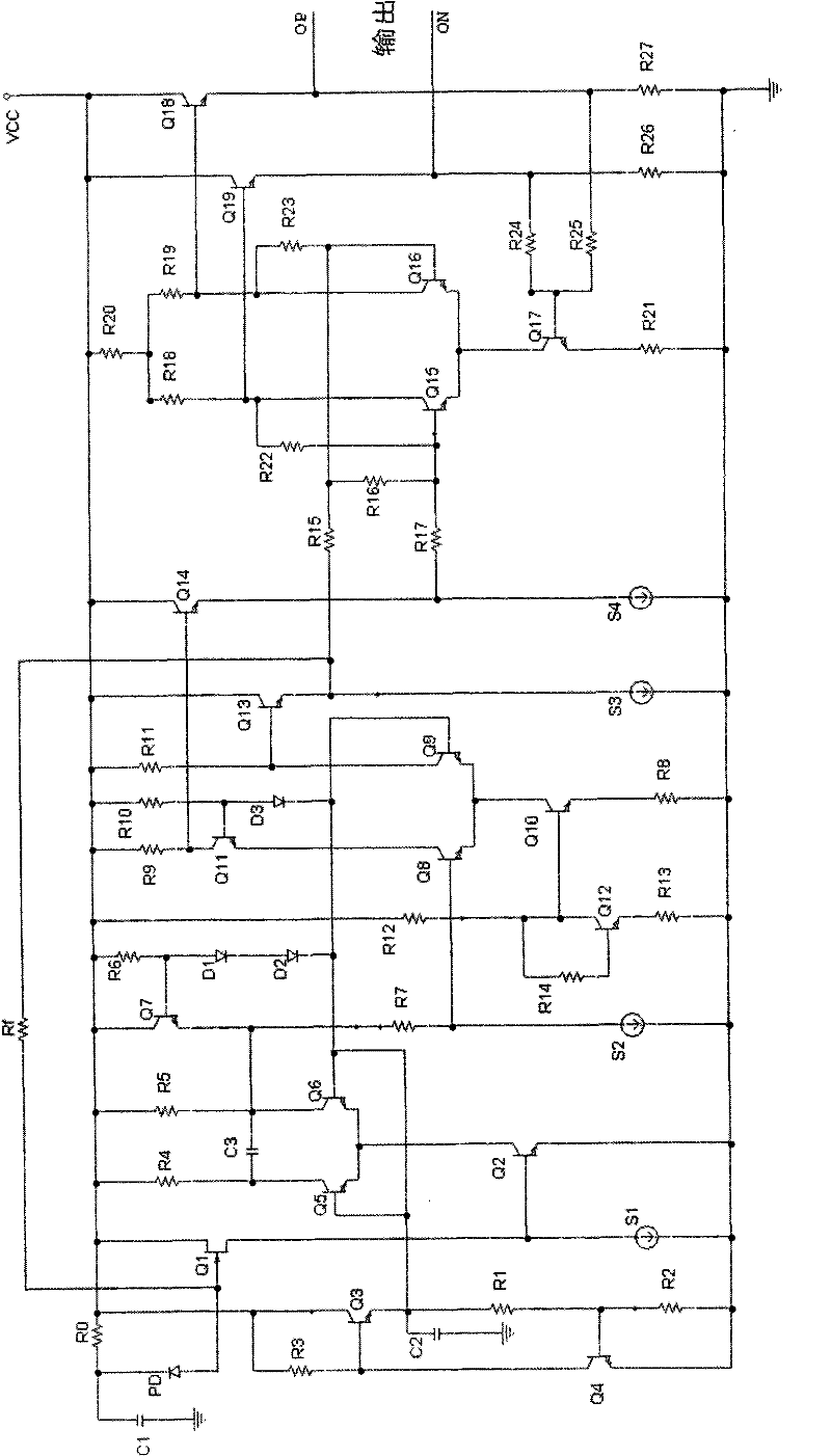
Figure 2 
Figure 3
Abstract
Description
technical field
[0001] The invention relates to the field of optical communication receiving, in particular to an optical input preamplifier used in an optical communication receiver. Background technique
[0002] Generally, the role of the optical input preamplifier used in optical communication receivers in optical communication systems is to convert optical signals into electrical signals, and it generally consists of a photodiode (PD) and a transimpedance amplifier (TIA), where , the photodiode converts the received optical signal into a current signal, and then converts it into a voltage signal through a transimpedance amplifier and amplifies the output. Since the transimpedance gain and noise characteristics of the optical input preamplifier are important technical indicators that determine the receiving sensitivity of the optical receiver, the optical input preamplifier is one of the core components of the optical receiving and optical communication system.
[0003] ...
Examples
Embodiment Construction
[0033] Preferred embodiments of the present invention will be described in detail below in conjunction with the accompanying drawings.
[0034] Please refer to figure 1 , the optical input preamplifier for optical communication receiver provided by the present invention comprises a photodiode 1, a feedback resistor (Rf) 2, a reach by field effect transistor (FET) and bipolar transistor (BT) Linton circuit 3, a current-driven common base amplifier circuit 4, a differential amplifier circuit 5, a bias circuit 6 providing bias voltage, and a differential amplifier circuit 7 with voltage negative feedback.
[0035] The photodiode 1 converts the received light signal into a current signal, and the current signal is converted into a voltage signal through the feedback resistor 2 . The FET-BT Darlington circuit 3 converts the above-mentioned voltage signal into a current signal with a very high transconductance, and injects the current signal into the current-driven common base ampl...